 ALLPCB


Optimizing Solder Paste Application with Glossy Solder Masks: Best Practices
Solder paste application remains a critical step in surface mount technology assembly. The choice of solder mask finish influences how paste releases from the stencil and how it behaves during reflow. Glossy solder masks present specific surface characteristics that engineers must account for when setting up printing parameters. Proper optimization helps reduce defects such as bridging, insufficient solder, and tombstoning while maintaining consistent deposit volumes across panels.
Why Glossy Solder Masks Matter in SMT Processes
A solder mask protects copper traces and defines pad openings on printed circuit boards. Glossy finishes produce a smoother, higher-gloss surface compared with matte alternatives. This smoothness can improve paste release from fine apertures but may also alter the contact angle between paste and mask. In high-volume SMT lines, these differences affect first-pass yield and rework rates. Engineers therefore adjust stencil design and printing settings to match the mask finish rather than applying generic parameters.
Technical Principles of Paste Behavior on Glossy Surfaces
Solder paste consists of alloy particles suspended in flux. During stencil printing, the paste must shear cleanly at the aperture walls and transfer fully to the pad. A glossy mask reduces surface roughness, which lowers mechanical interlocking between paste and mask. This can improve release efficiency when aperture aspect ratios are high. However, the same smoothness may increase the risk of paste sliding if squeegee pressure or speed is not balanced correctly. Reflow dynamics also change slightly because the glossy surface affects how flux spreads before the alloy melts. Consistent control of print parameters therefore becomes essential to avoid volume variation.
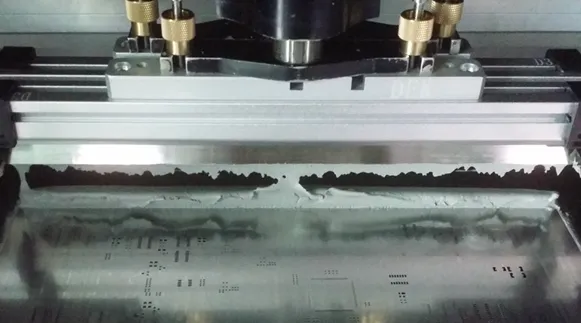
Stencil Design Adjustments for Glossy Masks
Stencil thickness and aperture geometry directly influence paste volume. For glossy masks, designers often reduce aperture area slightly compared with matte-mask designs to compensate for improved release. Trapezoidal or stepped apertures can further enhance transfer efficiency on smooth surfaces. Engineers verify these choices through test prints before committing to production tooling. IPC-7525 provides guidance on stencil design considerations that apply across different mask finishes.
Paste type selection also plays a role. Finer particle sizes in the paste formulation help fill small apertures more reliably when the mask is glossy. Flux activity level must remain compatible with the reflow profile to prevent oxidation on the smooth pad surfaces. Trial runs on actual production panels confirm whether the chosen combination meets volume targets.
Printing Process Best Practices and Parameter Tuning
Squeegee pressure, speed, and angle require fine-tuning when glossy masks are in use. Lower pressure often suffices because the smooth surface reduces friction, yet insufficient pressure can leave paste on the stencil. Speed adjustments prevent the paste from rolling rather than shearing cleanly. Separation speed after printing also merits attention; a controlled peel rate minimizes tailing on glossy finishes.
Support tooling such as vacuum tables or dedicated fixtures helps maintain board flatness. Warpage during printing can distort deposit shapes regardless of mask finish. Regular inspection of the first few boards from each setup catches issues before they propagate through the line.
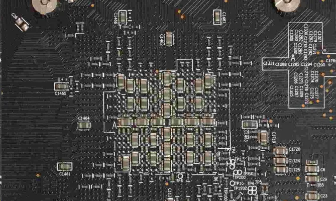
Reflow Considerations and Defect Troubleshooting
During reflow, the glossy mask surface influences flux flow and alloy wetting. Profiles developed for matte masks may need minor adjustments to peak temperature or soak time. Too rapid a ramp can cause paste to slump before full wetting occurs. Monitoring the process with thermal profiling tools confirms that every zone stays within acceptable limits for the specific paste and mask combination.
Common defects include bridging between closely spaced pads and insufficient volume on larger pads. Increasing aperture reduction or switching to a different paste viscosity often resolves these issues. Tombstoning may appear when one end of a component lifts due to uneven paste volume; balancing deposit height across pads corrects the imbalance. Systematic troubleshooting begins with print inspection data rather than reflow adjustments alone.
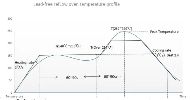
Conclusion
Optimizing solder paste application for glossy solder masks centers on matching stencil design, printing parameters, and reflow settings to the smoother surface characteristics. Attention to release efficiency, deposit volume consistency, and thermal profiling reduces defects and improves overall process capability. These practices align with established guidelines such as those in J-STD-005 for solder paste and IPC-A-610 for assembly acceptance criteria.
FAQs
Q1: How does a glossy solder mask affect solder paste release during stencil printing?
A1: A glossy finish reduces surface roughness, which generally improves paste release from stencil apertures compared with matte masks. Engineers may need to adjust aperture size or separation speed to maintain target volumes. Consistent test printing verifies the settings for each specific board design.
Q2: What stencil design changes help when using glossy solder masks in SMT assembly?
A2: Designers often apply modest aperture reductions and consider trapezoidal wall profiles to optimize transfer on smooth surfaces. These modifications account for the lower mechanical interlocking between paste and mask. Verification through production-representative test prints confirms acceptable results.
Q3: Which reflow adjustments are typically required with glossy solder masks?
A3: Minor changes to ramp rate or peak temperature can prevent slumping or incomplete wetting on the smoother mask surface. Thermal profiling on actual assemblies ensures the profile stays compatible with the chosen paste. Monitoring deposit behavior during initial runs identifies any needed tweaks.
Q4: How can engineers troubleshoot bridging when printing on glossy masks?
A4: Bridging often stems from excess paste volume or insufficient separation control. Reducing aperture area or lowering squeegee pressure frequently resolves the issue. Reviewing print inspection data before reflow helps isolate whether the root cause lies in printing or later process steps.
References
IPC-7525B — Stencil Design Guidelines. IPC, 2019
J-STD-005A — Requirements for Soldering Pastes. IPC, 2016
IPC-A-610G — Acceptability of Electronic Assemblies. IPC, 2017





