 ALLPCB


Solar inverters convert direct current from photovoltaic panels into alternating current for grid or load use. The printed circuit board layout directly influences conversion efficiency, heat generation, and electromagnetic compatibility. Engineers focus on solar inverter PCB layout optimization to reduce resistive and switching losses while maintaining reliable operation under varying load and environmental conditions. High-efficiency PCB design practices address current-carrying capacity, thermal paths, and signal integrity simultaneously. These considerations become critical in systems rated from a few kilowatts to hundreds of kilowatts, where even small percentage-point improvements in efficiency translate into meaningful energy yield over the inverter lifetime.
Why Solar Inverter PCB Layout Optimization Matters
In solar inverters, power losses occur primarily through conduction in traces and components, switching transitions in semiconductors, and parasitic effects such as stray inductance and capacitance. Poor layout increases these losses, raising operating temperatures and reducing overall system efficiency. Effective thermal management PCB design keeps junction temperatures within safe limits, extending component life and preventing derating. EMI reduction in inverter PCBs prevents interference with control circuits and compliance with regulatory limits. When layout decisions are made early, the resulting board supports higher power density without compromising reliability or requiring excessive heatsinking.
Technical Principles of Power Loss and Efficiency in Inverter PCBs
Conduction losses follow the relationship between current and trace resistance, where resistance depends on copper thickness, width, and length. Longer or narrower traces increase voltage drop and heat generation, particularly in the DC link and output stages carrying high currents. Switching losses arise during the turn-on and turn-off intervals of power devices; parasitic inductance in the commutation loop prolongs these transitions and generates voltage spikes. Thermal resistance from junction to ambient determines how effectively heat dissipates through the board, vias, and copper planes. Electromagnetic interference originates from rapid current changes that create magnetic fields and from voltage changes that create electric fields; loop area and return paths strongly influence radiated and conducted emissions.
(Insert image: 'High-Current Trace Layout Comparison' · ALT: 'Side-by-side PCB layouts showing wide versus narrow traces for high-current paths in solar inverters')
Mechanisms of Thermal and EMI Challenges
Heat generated in power semiconductors and inductors conducts through the board dielectric and spreads via copper planes. Insufficient thermal vias or inadequate plane area creates hot spots that accelerate aging and may trigger thermal shutdown. EMI coupling occurs through shared return paths, capacitive coupling between adjacent traces, and inductive coupling in current loops. High-frequency harmonics from pulse-width modulation exacerbate these effects, potentially violating conducted and radiated emission limits. Ground plane discontinuities or improper partitioning between power and control sections allow noise to propagate into sensitive feedback and gate-drive circuits.
Best Practices for High-Efficiency PCB Design
Place power semiconductors and magnetics close together to minimize commutation loop inductance while maintaining adequate creepage and clearance distances. Route high-current traces on outer layers with maximum copper weight and use multiple vias to transfer current to inner planes when needed. Implement solid ground planes beneath power stages and employ star-point grounding or controlled impedance returns for control signals. Position gate-drive components near their respective switches to shorten drive loops and reduce ringing. Separate analog sensing circuits from high-voltage switching areas by distance and shielding where possible.
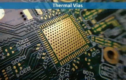
Thermal Management PCB Design Techniques
Distribute heat-generating components to avoid localized temperature rise and align them with airflow or heatsink mounting locations. Use thick copper planes and arrays of thermal vias to lower thermal resistance from component pads to the board underside or heatsink. Select board materials with appropriate glass-transition temperature and thermal conductivity for the expected operating range. Ensure that copper balance on both sides of the board minimizes warpage during thermal cycling. Verify that via fill or plating processes maintain structural integrity under repeated thermal stress.
EMI Reduction in Inverter PCBs
Minimize the area of high-frequency current loops by placing decoupling capacitors close to power device terminals. Route differential pairs for current sensing with tight coupling and controlled impedance. Apply stitching vias along plane edges to contain return currents and reduce slot radiation. Incorporate input and output filters with proper layout to prevent noise bypassing. Partition the board into power, control, and interface zones with ground plane cuts only where necessary for isolation.
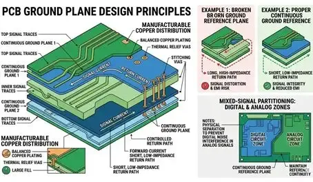
Practical Component Placement and Routing Guidelines
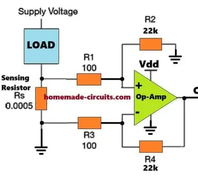
Position the DC-link capacitor bank centrally relative to the half-bridge or full-bridge legs to equalize parasitic inductance across phases. Route gate signals on dedicated layers with adjacent return paths and avoid crossing high-current traces. Place current-sense resistors or shunts in low-inductance configurations and keep associated amplifier circuitry nearby. Maintain consistent trace widths based on current-carrying requirements and temperature rise limits. Review the entire layout for mechanical constraints such as mounting holes and connector placement that may affect electrical performance.
Conclusion
Optimizing solar inverter PCB layout for maximum efficiency requires simultaneous attention to conduction paths, thermal dissipation, and electromagnetic compatibility. Structured placement, appropriate copper distribution, and careful return-path design reduce power losses and improve reliability. Adherence to established industry standards ensures consistent quality and performance across production volumes. Engineers who apply these principles early in the design cycle achieve higher conversion efficiency and lower operating costs over the system lifetime.
FAQs
Q1: How does solar inverter PCB layout optimization improve overall system efficiency?
A1: Solar inverter PCB layout optimization reduces resistive voltage drops and parasitic inductance in high-current paths, lowering conduction and switching losses. Shorter, wider traces and optimized component placement decrease heat generation, allowing the inverter to operate closer to its theoretical maximum efficiency. Thermal management PCB design further supports sustained performance by keeping semiconductor junctions within rated temperature ranges.
Q2: What role does thermal management PCB design play in minimizing power loss in solar inverters?
A2: Thermal management PCB design lowers the thermal resistance between power devices and the ambient environment through copper planes, thermal vias, and strategic component spacing. Reduced junction temperatures decrease on-state resistance of semiconductors and prevent efficiency derating at elevated ambient conditions. Effective heat spreading also improves long-term reliability by slowing degradation mechanisms driven by temperature.
Q3: How can EMI reduction in inverter PCBs be achieved during the layout stage?
A3: EMI reduction in inverter PCBs begins with minimizing current-loop areas, providing continuous return planes, and separating noisy power sections from sensitive control circuitry. Proper decoupling, controlled-impedance routing, and stitching vias contain high-frequency currents and limit radiation. These layout choices help meet regulatory emission limits without requiring excessive external filtering components.
Q4: Why is high-efficiency PCB design particularly important for solar inverter applications?
A4: High-efficiency PCB design directly affects the energy yield of a photovoltaic installation because even small efficiency gains accumulate over thousands of operating hours. Lower losses reduce cooling requirements and allow higher power density within the same enclosure volume. Consistent application of layout best practices also supports compliance with safety and performance standards across varying environmental conditions.
References
IPC-2221B — Generic Standard on Printed Board Design. IPC, 2012
IPC-6012E — Qualification and Performance Specification for Rigid Printed Boards. IPC, 2017
IPC-A-600K — Acceptability of Printed Boards. IPC, 2020





