 ALLPCB


Introduction
Printed circuit board designers face increasing pressure to pack more functionality into smaller spaces, making PCB routing techniques essential for success. High-density interconnects demand innovative approaches to overcome routing congestion and layer stackup limitations. Via filling emerges as a key strategy in PCB design optimization, enabling traces to route directly over vias without gaps or obstructions. This method supports reducing layer count by maximizing available routing area on each layer. Engineers benefit from improved signal integrity and thermal management as filled vias enhance overall board reliability. By integrating via placement strategies early, designs achieve higher routing density while adhering to manufacturability constraints.
Understanding Via Filling in PCB Routing
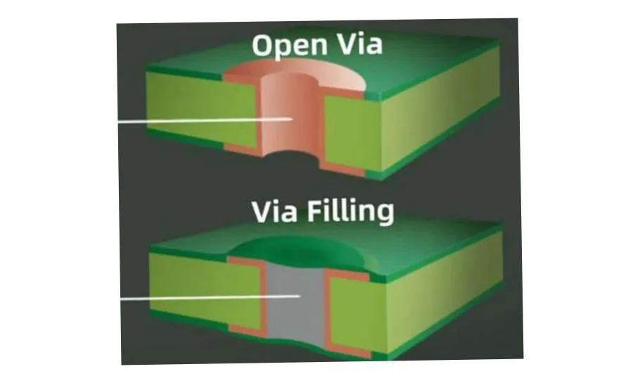
Via filling involves completely or partially filling drilled vias with conductive or non-conductive materials to prepare the surface for subsequent routing or component placement. In standard through-hole vias, the open barrel creates a barrier for traces, limiting PCB routing techniques on adjacent areas. Filling eliminates this issue, allowing via-in-pad configurations that are vital for ball grid array components and fine-pitch devices. Non-conductive fills, such as epoxy resins, provide mechanical support and prevent contamination, while conductive fills like electroplated copper maintain electrical continuity. This process aligns with industry needs for compact electronics in telecommunications and computing applications. Proper via filling directly contributes to increasing routing density by reclaiming surface real estate.
The relevance of via filling grows with the adoption of high-density interconnect boards, where layer transitions must support dense trace patterns. Unfilled vias force detours in routing paths, escalating layer counts to resolve congestion. Filled vias planarize the surface, enabling seamless trace continuity across layers. Engineers must consider fill type based on electrical, thermal, and mechanical requirements during initial layout planning. This approach not only streamlines PCB design optimization but also reduces fabrication complexities associated with multiple layers.
Technical Principles of Via Filling
Via filling relies on precise material deposition to achieve void-free structures, governed by electrochemical or mechanical processes. Conductive filling uses pulse reverse electroplating, where copper ions deposit from bottom to top, minimizing voids through controlled current reversal. This superfilling technique ensures uniform conductivity comparable to solid copper traces. Non-conductive filling employs screen-printed or vacuum-injected epoxy pastes that cure to form a stable plug. Both methods require post-fill planarization via grinding or lapping to maintain flatness for solder mask application. These principles underpin reliable interlayer connections in multilayer boards.
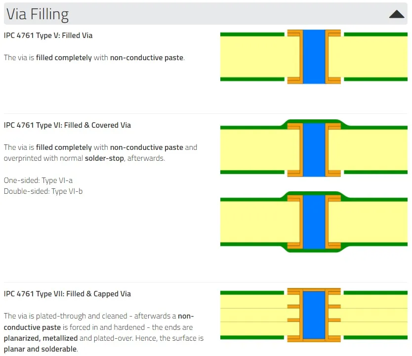
IPC-4761 outlines via protection types, including Type VI-B for filled and covered vias, specifying coverage and fill completeness for design integrity. The standard emphasizes protection against environmental factors like moisture ingress, which unfilled vias are prone to. In high-aspect-ratio vias, fill processes must account for material flow dynamics to avoid air entrapment. Thermal expansion mismatches between fill materials and copper plating demand careful selection to prevent cracking during reflow. Electrical performance improves as filled vias reduce inductance in high-speed signals. Mechanical strength increases, supporting via placement strategies in stress-prone areas.
Aspect ratios influence fill feasibility, with microvias under 0.25 mm depth benefiting most from these techniques. Laser-drilled vias pair effectively with conductive fills for high-density interconnects. Process control ensures at least partial fill to meet acceptance criteria, preventing plating separation. Integration into stackups allows blind and buried vias to further optimize layer usage.
Via Filling Techniques and Via Placement Strategies
Several PCB routing techniques leverage via filling, starting with via-in-pad for dogbone escapes under BGAs. Strategic via placement clusters vias in power/ground planes to minimize signal interference while maximizing fill efficiency. Staggered arrays reduce fill material bridging risks during injection. For reducing layer count, combine filled microvias with any-layer interconnects to shorten escape routes. Placement near component pads shortens traces, aiding impedance control. These strategies enhance overall PCB design optimization.
Conductive filling suits power distribution nets due to low resistance paths. Non-conductive options suffice for signal vias where planarity is paramount. Best practices include specifying fill direction and post-planarization tolerances in fabrication notes. Avoid overfilling to prevent dome formation, which complicates solder mask registration. Simulate thermal profiles to validate fill integrity under assembly conditions. Layer pairing dictates via depth, influencing fill method selection.
IPC-6012 provides qualification criteria for filled vias, including void limits and plating thickness uniformity. Compliance ensures boards withstand environmental stresses without delamination. Engineers should prototype via farms to verify fill quality before full-panel production.
Best Practices for PCB Design Optimization with Filled Vias
Implement via placement strategies by grouping vias by function: signal vias in inner layers, power vias filled conductively on outer planes. Minimize via diameters to 0.15 mm where possible, balancing drill accuracy with fill challenges. Route critical nets first, using filled vias to fanout high-pin-count devices efficiently. This PCB routing technique preserves outer layers for shielding. Employ teardrop pads to reduce stress concentrations around filled vias. Iterative DRC checks confirm spacing rules for post-fill traces.
To achieve increasing routing density, limit unfilled vias to non-critical areas. Hybrid stackups with filled blind vias reduce transitions, directly supporting reducing layer count from 12 to 8 in many designs. Thermal vias under hotspots benefit from conductive fills for heat spreading. Document fill requirements explicitly to align with fabricator capabilities. Post-layout analysis tools verify routing efficiency gains.
Challenges include cost premiums for filling processes and potential voids in high-aspect vias. Mitigate by selecting low-viscosity epoxies and optimizing cure cycles. Reliability testing per IPC standards validates long-term performance. Collaboration with manufacturers refines via placement strategies for yield.
Benefits and Implementation Insights
Filled vias enable tighter BGA pitches by eliminating solder wicking risks during assembly. Routing density surges as traces cross former via sites, freeing space for additional nets. Layer count reductions lower material costs and simplify fabrication. Electrical conductivity rivals solid planes in conductive fills, ideal for high-current paths. Mechanical robustness improves board warp resistance under thermal cycling. These advantages position via filling as a cornerstone of modern PCB design optimization.
In practice, transition from 4-layer to 2-layer prototypes using filled vias demonstrates feasibility. Monitor impedance with field solvers incorporating fill properties. Scale to production by validating cross-sections for fill completeness.
Conclusion
Via filling transforms PCB routing techniques by enabling via-in-pad layouts that boost density and trim layers. Strategic via placement and fill selection drive PCB design optimization for compact, reliable boards. Adhering to standards like IPC-4761 and IPC-6012 ensures manufacturability and performance. Engineers gain flexibility in high-stakes applications through these methods. Future designs will increasingly rely on advanced filling for next-generation interconnects.
FAQs
Q1: What are effective PCB routing techniques using via filling?
A1: Via filling supports via-in-pad routing, allowing traces to cross filled vias for denser patterns. Combine with blind vias and staggered placement to minimize layer transitions. This increases routing density while maintaining signal integrity. Follow IPC-4761 for protection types to ensure reliability. Practical implementation involves early specification of fill materials.
Q2: How does via filling help in reducing layer count?
A2: Filled vias eliminate routing blockages, enabling more traces per layer and shortening interconnect paths. Designers consolidate functions across fewer layers by using via-in-pad for escapes. This PCB design optimization reduces stackup thickness and cost. Non-conductive fills provide planarity for outer layer routing. Validation through stackup simulations confirms layer savings.
Q3: What via placement strategies improve routing density?
A3: Cluster vias by net class, prioritizing filled vias under components for short escapes. Stagger arrays to aid fill processes and use microvias for inner layers. Integrate with fanout patterns for BGAs to maximize space. These strategies enhance PCB routing techniques in high-density boards. DRC enforcement prevents overlaps.
Q4: Why is PCB design optimization critical with filled vias?
A4: Optimization ensures void-free fills and planar surfaces, preventing assembly defects. Balances electrical, thermal, and mechanical needs through material choice. Reduces layer count and boosts density for compact devices. Standards like IPC-6012 guide acceptance. Prototyping refines strategies for production yields.
References
IPC-4761 — Design Guide for Protection of Printed Board Via Structures. IPC, 2006
IPC-6012E — Qualification and Performance Specification for Rigid Printed Boards. IPC, 2017


