ALLPCB


Introduction
In advanced electronics, high-density interconnect (HDI) printed circuit boards rely heavily on microvias to achieve compact designs and superior signal integrity. These small vias, typically under 150 microns in diameter, enable connections between closely spaced layers, supporting the miniaturization demands of smartphones, wearables, and automotive systems. However, microvia PCB reliability becomes a critical concern due to thermal stress encountered during assembly and operation. Thermal mismatches between materials generate stresses that can lead to failures over time. Engineers must address these challenges to ensure long-term performance in harsh environments. This article explores microvia thermal stress mechanisms, failure analysis techniques, and proven strategies aligned with industry standards.
Understanding Microvias and Their Role in HDI PCBs
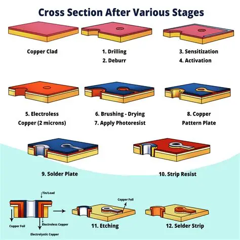
Microvias are blind or buried vias formed by laser drilling or sequential lamination, distinguishing them from standard through-holes in size and aspect ratio. They facilitate higher routing density, allowing finer pitch components like BGAs to connect efficiently across layers. In HDI constructions, microvias support build-up processes that stack or stagger vias to span multiple layers. While they offer electrical advantages, their small size amplifies vulnerability to mechanical and thermal loads. Factory processes must prioritize reliability to prevent field failures in production-scale boards. Adhering to established design rules ensures microvias withstand real-world conditions.
Why Microvia Thermal Stress Matters for Reliability
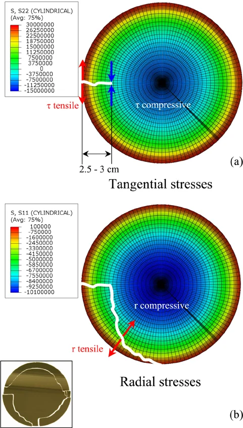
Thermal stress arises primarily from coefficient of thermal expansion (CTE) differences between copper plating and the surrounding dielectric resin. During reflow soldering or operational temperature swings, the board expands and contracts unevenly, concentrating shear forces at the via interface. This leads to PCB microvia reliability issues, such as pad lifts or barrel cracks, especially in multilayer stacks. In advanced electronics, repeated cycles accelerate fatigue, compromising signal paths and overall board functionality. Engineers observe higher failure rates in densely packed designs without mitigation. Proactive management of these stresses directly impacts product lifespan and yield.
Mechanisms of Thermal Stress in Microvias
The core mechanism involves thermo-mechanical strain from CTE mismatch, where copper (CTE around 17 ppm/°C) contrasts with organic dielectrics (higher Z-axis CTE). Laser-drilled microvias, often filled with conductive or non-conductive materials, experience peak stresses at corners and transitions during heating. In stacked configurations, cumulative loading from overlying vias exacerbates deformation. Thermal cycling simulates these conditions, revealing microcracks that propagate under sustained use. Material selection influences stress distribution, with low-CTE resins reducing peak strains. Understanding these dynamics guides robust factory implementations.
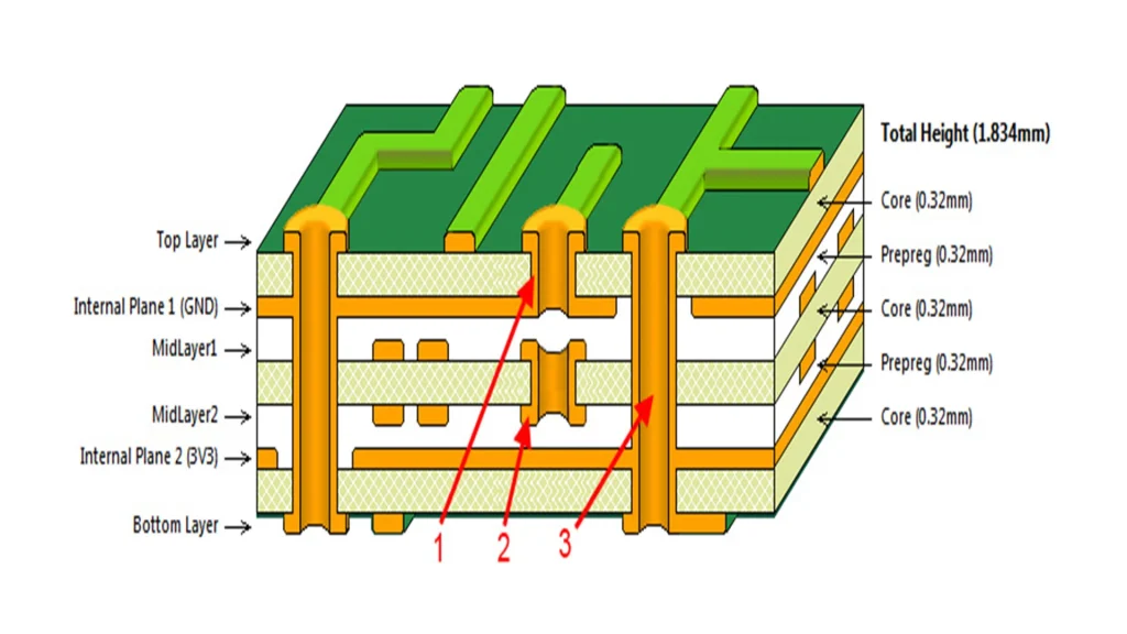
Staggered vs Stacked Microvias: A Reliability Comparison
Stacked microvias align vertically, one atop another, maximizing density but accumulating vertical stress that risks separation at interfaces. Staggered microvias offset each level, distributing loads horizontally and vertically for better strain relief. Factory data consistently shows staggered designs surviving more thermal cycles due to reduced alignment-induced weaknesses. IPC microvia standards, such as IPC-2226, outline HDI classes favoring staggered for extended layer counts beyond two. While stacked suits ultra-dense two-layer spans, staggering enhances PCB microvia reliability in demanding applications. Designers balance density needs with this trade-off during stack-up planning.
- Density: Stacked offers higher vertical interconnect; staggered provides moderate, offset routing.
- Stress distribution: Stacked concentrates axial stress; staggered disperses loads stepwise.
- Thermal cycle endurance: Stacked is more prone to cracking; staggered shows better fatigue resistance.
- Typical use: Stacked suits 1-2 layer spans; staggered is preferred for multi-layer HDI builds.
- Manufacturing complexity: Stacked requires critical sequential lamination; staggered allows easier alignment tolerance.
Common Failure Modes in Microvia Thermal Stress
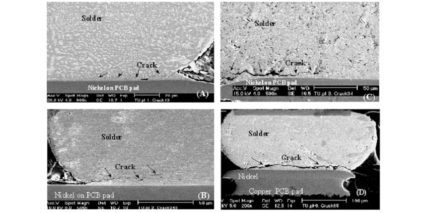
Primary failures include cracking at the copper-dielectric interface, void formation in fills, and pad cratering from delamination. Thermal expansion pushes plated walls outward, initiating fatigue cracks that open under cycling. Epoxy-filled vias may pump resin during heating, weakening barrels. In high-layer-count boards, stacked microvias show higher incidence due to compounded effects. Electrical opens manifest after hundreds of cycles, often undetectable until cross-sectioned. These modes underscore the need for rigorous process controls in fabrication.
Microvia Failure Analysis Techniques
Microvia failure analysis starts with electrical monitoring via daisy-chain coupons during accelerated thermal cycling. Non-destructive methods like X-ray reveal voids or misalignment before dissection. Cross-sectioning followed by scanning electron microscopy (SEM) identifies crack origins, such as plating voids or resin separation. Resistance changes per IPC-TM-650 test methods signal early degradation. Dye-and-peel tests expose interfacial lifts efficiently. Combining these provides root-cause insights, informing design refinements.
IPC Microvia Standards for Design and Qualification
IPC-2226 provides sectional guidelines for HDI, specifying microvia diameters, aspect ratios up to 1:1, and a preferred 0.75:1 for plating integrity. It classifies HDI types from passive to active, dictating via strategies per layer count. Qualification follows IPC-6016, mandating performance under thermal shock and cycling. These standards ensure factory consistency, with test vehicles verifying compliance. Aspect ratios prevent plating defects that amplify thermal vulnerabilities. Compliance minimizes risks in high-volume production.
Best Practices to Enhance Microvia Reliability
Select low-CTE, high-Tg dielectrics to match copper expansion and resist softening during reflow. Opt for staggered over stacked microvias when spanning more than two layers to distribute stresses. Increase via diameters and pad sizes within IPC-2226 limits for robust anchoring. Copper filling outperforms epoxy in thermal matching, reducing crack propagation. Thicker plating, minimum 20 microns, bolsters barrel strength against shear. Implement sequential lamination with precise registration to avoid misalignment.
Precondition boards per JEDEC moisture sensitivity levels before thermal stress testing. Conduct interconnect stress tests (IST) simulating field cycles. Monitor via resistance dynamically to catch anomalies early. Factory validation uses dedicated coupons for statistical confidence. These practices yield reliable HDI boards for advanced electronics.
Troubleshooting Thermal Stress Failures
When failures occur, review stack-up for excessive stacking without offsets. Analyze reflow profiles for peak temperatures exceeding material limits. Inspect drilling quality, as rough walls promote stress risers. Simulate via stresses using finite element models to predict weak points. Adjust fill materials if voids appear post-cycling. Iterative testing refines processes, aligning with IPC qualification.
Conclusion
Microvia PCB reliability hinges on mitigating thermal stress through informed design and manufacturing. Staggered configurations, standard-compliant aspect ratios, and robust materials address CTE mismatches effectively. Failure analysis tools enable precise diagnostics, while best practices ensure endurance. By integrating IPC microvia standards, engineers achieve dependable HDI performance. Prioritizing these strategies supports innovation in compact electronics without compromising longevity.
FAQs
Q1: What causes microvia thermal stress in PCBs?
A1: Microvia thermal stress stems from CTE mismatches between copper plating and dielectric materials during temperature changes. Reflow soldering and operational cycling induce shear at interfaces, leading to cracks. Factory preconditioning and low-CTE laminates mitigate this. Proper via filling prevents void-induced failures. Adhering to IPC guidelines enhances overall PCB microvia reliability.
Q2: How do staggered microvias improve reliability over stacked ones?
A2: Staggered microvias offset layers, distributing thermal loads stepwise rather than axially. This reduces fatigue at single points, surviving more cycles in testing. Stacked versions concentrate stresses, risking separation in multilayers. IPC-2226 recommends staggering for complex HDI. Designers gain density with reliability trade-offs.
Q3: What role do IPC microvia standards play in thermal reliability?
A3: IPC-2226 defines HDI design rules like aspect ratios for plating quality and stress resistance. IPC-6016 qualifies boards under thermal conditions. These ensure consistent fabrication. Compliance verifies microvia thermal stress tolerance via standardized tests.
Q4: How is microvia failure analysis performed under thermal stress?
A4: Analysis uses daisy-chain resistance monitoring during cycling per IPC-TM-650. Cross-sections and SEM reveal cracks. X-ray detects voids non-destructively. Root causes like CTE mismatch guide fixes. This process optimizes future builds.
References
IPC-2226A - Sectional Design Standard for High Density Interconnect Printed Boards. IPC, 2017
IPC-6016D - Qualification and Performance Specification for High Density Interconnect Printed Boards. IPC, 2019
IPC-TM-650 - Test Methods Manual. IPC
JEDEC JESD22-A104 - Temperature Cycling. JEDEC