 ALLPCB


Introduction
Wearable health devices require printed circuit boards that deliver advanced sensing, processing, and wireless capabilities within extremely limited footprints. Engineers address this challenge through systematic miniaturization approaches that maintain electrical performance and mechanical reliability. Techniques such as high density interconnect construction and system in package integration enable the placement of more components in smaller areas without compromising signal integrity. These strategies support continuous monitoring functions in devices worn directly on the body for extended periods. The result is improved user comfort alongside expanded diagnostic features in health applications.
Why Miniaturization Matters in Wearable Health Electronics
Compact PCB designs directly influence the size, weight, and battery life of wearable health products. Smaller boards allow devices to fit unobtrusively on wrists, patches, or clothing while incorporating multiple sensors and communication modules. This capability proves essential for applications that track vital signs over long durations without frequent recharging. Component miniaturization techniques PCB approaches also reduce material usage and support higher production volumes in medical electronics. Overall, these methods help meet the growing expectations for multifunctional yet discreet health monitoring solutions.
Technical Principles of HDI PCB Wearable Health Designs
High density interconnect technology forms the foundation for achieving greater circuit density in constrained spaces. Microvia technology wearable implementations use laser-drilled vias with diameters typically below 150 micrometers to create vertical connections between layers. This approach replaces larger through-hole vias and frees surface area for additional components. Stacked or staggered microvia arrangements further increase routing density while preserving controlled impedance for high speed signals. Engineers apply these principles to route power, ground, and data lines efficiently across multiple layers in flexible or rigid flex constructions suited to body worn devices.
Dense component placement PCB strategies rely on fine pitch land patterns and optimized pad geometries to accommodate smaller packages. Thermal management considerations remain critical because reduced board area concentrates heat from active components. Designers evaluate copper thickness, via fill materials, and layer stackups to dissipate heat without adding bulk. Reliability under flexing and environmental exposure follows established qualification procedures that verify performance across temperature cycles and mechanical stress.
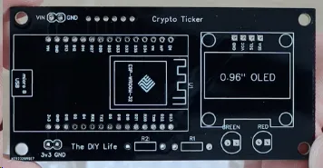
Component Miniaturization Techniques and SiP for Wearable Devices
Component miniaturization techniques PCB include selection of chip scale packages, wafer level packages, and bare die attachments where appropriate. These options reduce the lateral dimensions of integrated circuits and passive devices compared with traditional surface mount formats. Passive components in 01005 or smaller case sizes further contribute to space savings when electrical requirements permit. Careful attention to placement rules prevents tombstoning or bridging during assembly of these fine pitch parts.
SiP for wearable devices integrates multiple dies, passives, and sometimes sensors into a single module that functions as a complete subsystem. This method reduces the number of discrete components on the main board and shortens interconnect lengths for improved signal quality. Package on package stacking represents another variant that adds vertical density without expanding the board outline. Engineers evaluate thermal interfaces and mechanical attachment methods to ensure the combined assembly withstands repeated flexure and moisture exposure typical in health wearables.
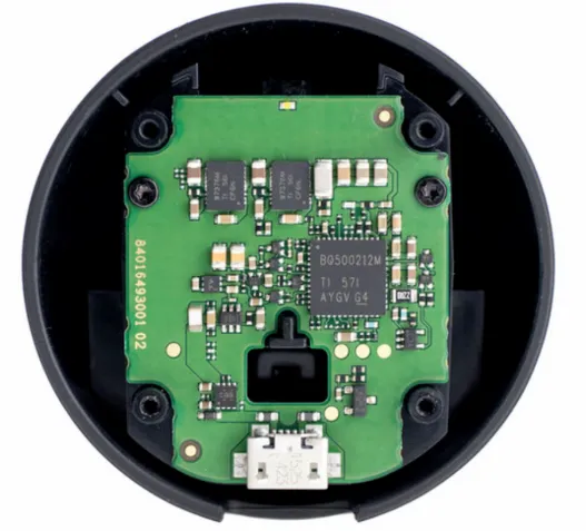
Practical Solutions and Best Practices for Dense Integration
Design teams begin with a thorough stackup analysis that balances layer count, dielectric thickness, and via aspect ratios to achieve target densities. Sequential lamination processes enable the formation of reliable microvia structures while controlling warpage in thin constructions. Placement optimization software assists in arranging components to minimize trace lengths and avoid routing congestion in high speed sections. Ground planes and power distribution networks receive particular attention to maintain low impedance paths despite the reduced board area.
Assembly considerations include solder paste volume calculations for small pads and reflow profile adjustments that accommodate mixed component sizes. Inspection methods such as automated optical inspection and X ray imaging verify joint quality on hidden interconnects. Testing protocols incorporate bend and twist evaluations along with environmental conditioning to confirm long term durability in wearable use cases.
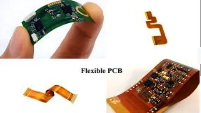
Reliability and Quality Considerations
Industry standards guide the qualification of miniaturized boards to ensure consistent performance. IPC 6012E outlines requirements for rigid printed boards that apply to the base materials and via structures used in these designs. Separate evaluations address the unique demands of flexible sections and component attachments under dynamic conditions. Thermal cycling and humidity exposure tests verify that microvia integrity and solder joint reliability meet application needs without introducing new failure modes.
Design for manufacturability reviews incorporate feedback from fabrication and assembly partners early in the process. This collaboration identifies potential issues with via fill, copper balancing, and panelization before committing to production tooling. Documentation of stackup details, material specifications, and acceptance criteria supports traceability throughout the supply chain.
Conclusion
Miniaturization strategies centered on HDI PCB wearable health constructions, microvia technology wearable features, component miniaturization techniques PCB, SiP for wearable devices, and dense component placement PCB enable engineers to deliver greater functionality in smaller form factors. Structured application of these methods, combined with adherence to relevant qualification standards, supports reliable operation in body worn health devices. Continued refinement of materials and processes will further expand the capabilities of compact electronics for medical monitoring.
FAQs
Q1: How does microvia technology wearable support higher component counts in health devices?
A1: Microvia technology wearable reduces via footprint size compared with traditional through holes, allowing more routing channels and component pads on each layer. This enables designers to place additional sensors and processors within the same board outline while maintaining signal integrity for health data transmission. The approach aligns with established fabrication guidelines for consistent via quality.
Q2: What role does SiP for wearable devices play in overall board miniaturization?
A2: SiP for wearable devices combines multiple functions into one module, decreasing the number of separate components that must be mounted on the main PCB. This consolidation shortens interconnect distances and frees surface area for other elements such as antennas or batteries. The resulting assembly maintains electrical performance suitable for continuous health monitoring applications.
Q3: Which component miniaturization techniques PCB help achieve dense placement without reliability trade offs?
A3: Component miniaturization techniques PCB involve selecting smaller package types and optimizing land patterns to fit more parts in limited space. Engineers apply spacing rules derived from assembly process capabilities and verify joint integrity through inspection methods. These steps support high density layouts while meeting mechanical and environmental requirements for wearable health products.
Q4: How do standards influence the design of HDI PCB wearable health boards?
A4: Standards such as those from IPC provide acceptance criteria for via structures, conductor spacing, and material performance that apply directly to HDI PCB wearable health constructions. They guide stackup development and qualification testing to ensure boards withstand flexure, temperature changes, and moisture typical in body worn use. Compliance documentation supports consistent manufacturing outcomes across production runs.
IPC-6012E — Qualification and Performance Specification for Rigid Printed Boards. IPC, 2017
JEDEC J-STD-020E — Moisture/Reflow Sensitivity Classification. JEDEC, 2014
IPC-A-600K — Acceptability of Printed Boards. IPC, 2020





