 ALLPCB


Why Compact Surveillance PCB Design Matters
Miniaturized PCB design addresses the core requirement of fitting advanced electronics into small form factors for security systems. Devices such as wireless cameras and motion detectors benefit from reduced board size that allows integration into everyday objects or tight enclosures. High-density PCB layout techniques support more components per unit area while maintaining signal integrity and thermal performance. Space-saving PCB solutions therefore contribute directly to the effectiveness of discreet monitoring equipment used by professionals in various sectors.
Industry standards guide these efforts to ensure consistency and reliability. IPC-6012E specifies qualification and performance requirements for rigid printed boards that apply to compact designs in demanding applications.
Technical Principles of High-Density PCB Layout
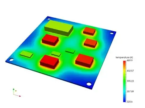
High-density interconnect technology forms the foundation of miniaturized PCB design by enabling finer traces and smaller vias than traditional methods. Engineers place components closer together while managing electromagnetic interference through careful routing and ground plane design. Multilayer constructions allow signal layers to be separated from power and ground planes which improves overall electrical performance in surveillance circuits. Thermal management becomes critical because reduced board area concentrates heat from active components such as processors and wireless modules.
Component selection also influences the final layout. Surface-mount devices with smaller footprints replace larger through-hole parts to achieve the necessary density. Microvia structures connect layers efficiently without consuming excessive board real estate. These approaches maintain the mechanical stability required for devices that may experience vibration or temperature cycling during operation.

Practical Solutions and Best Practices
Designers begin by defining strict constraints on board dimensions and component placement early in the project. Layer stack-up planning ensures adequate routing channels while controlling impedance for high-speed signals common in modern surveillance systems. Following established guidelines for via placement and trace width helps avoid manufacturing defects that could compromise reliability.
Assembly considerations include the use of appropriate solder masks and surface finishes that support fine-pitch components. Moisture sensitivity of parts must be addressed through proper handling and baking procedures before reflow. JEDEC J-STD-020E provides the classification framework for moisture and reflow sensitivity that helps engineers select and process components correctly in compact assemblies.
Testing protocols verify both electrical functionality and mechanical integrity after assembly. Automated optical inspection combined with electrical testing confirms that high-density layouts meet performance targets. These steps reduce the risk of field failures in security devices that operate continuously.

Additional Considerations for Quality and Reliability
Material selection plays a key role in achieving the required balance of electrical performance and mechanical strength. Laminates with appropriate dielectric constants and thermal expansion coefficients support stable operation across temperature ranges encountered in indoor and outdoor surveillance installations. IPC-A-600K outlines acceptability criteria for printed boards that serve as a reference during incoming inspection and final quality checks.
Design for manufacturability reviews help identify potential issues such as insufficient spacing or unbalanced copper distribution before production begins. These reviews incorporate feedback from fabrication and assembly partners to optimize yield on small boards. The result is a more robust product that meets the expectations of engineers responsible for deploying discreet surveillance solutions.
Conclusion
Compact PCB design enables the development of effective discreet surveillance devices through systematic application of high-density layout principles and adherence to recognized industry standards. Engineers achieve space savings while preserving signal integrity thermal performance and long-term reliability. Practical implementation involves careful component selection layer planning and quality verification at each stage. These practices support the creation of surveillance electronics that meet both functional and size requirements in professional applications.
FAQs
Q1: What advantages does a small PCB for security devices provide compared with larger alternatives?
A1: A small PCB for security devices allows integration into limited spaces while supporting essential functions such as imaging processing and wireless communication. Engineers achieve this through high-density PCB layout that places more components in less area without compromising electrical performance. The approach reduces overall device size and improves concealment options in surveillance installations.
Q2: How does compact surveillance PCB design affect device performance?
A2: Compact surveillance PCB design maintains signal integrity and thermal management through multilayer construction and precise component placement. Miniaturized PCB design reduces parasitic effects when executed correctly and supports reliable operation in continuous monitoring scenarios. Engineers apply space-saving PCB solutions to balance size constraints with the electrical requirements of modern security systems.
Q3: What role do industry standards play in miniaturized PCB design for surveillance equipment?
A3: Industry standards establish consistent criteria for board qualification fabrication and assembly that apply to compact designs. They guide engineers in selecting materials and processes that deliver the necessary reliability for security applications. Adherence to these standards helps ensure that high-density PCB layout meets performance expectations over the product lifecycle.
Q4: Which techniques support space-saving PCB solutions in discreet surveillance products?
A4: Techniques such as microvia implementation fine-pitch component placement and optimized layer stack-ups enable space-saving PCB solutions. These methods allow engineers to fit required circuitry into smaller areas while addressing signal integrity and heat dissipation needs. The resulting compact surveillance PCB supports the development of unobtrusive yet capable monitoring devices.
References
IPC-6012E — Qualification and Performance Specification for Rigid Printed Boards. IPC, 2017
IPC-A-600K — Acceptability of Printed Boards. IPC, 2020
JEDEC J-STD-020E — Moisture/Reflow Sensitivity Classification. JEDEC, 2014





