ALLPCB


Multi-sheet schematics have become essential for handling the increasing complexity of modern electronic systems. Engineers working on advanced projects frequently encounter designs that exceed the capacity of single-sheet representations. This approach allows clear organization of interconnected functional blocks while maintaining overall system coherence. Effective use of multi-sheet schematic PCB techniques supports better collaboration among team members and reduces the risk of errors during later stages of development.
What Is Multi-Sheet Schematic PCB and Why It Matters
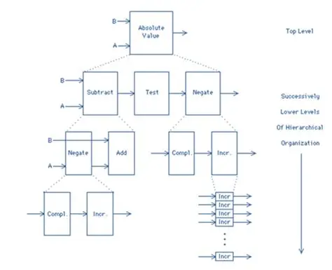
A multi-sheet schematic PCB consists of multiple interconnected drawing pages that together describe an entire circuit. Each sheet typically focuses on a specific subsystem such as power distribution, signal processing, or interface circuitry. Hierarchical schematic design builds on this structure by using top-level blocks that expand into detailed sub-sheets. Managing complex PCB schematics in this way becomes necessary when component counts rise into the thousands and signal paths span diverse functional areas. Large PCB schematic design projects benefit directly because engineers can isolate sections for focused review without losing sight of global connections. This method also improves version control and simplifies updates when specifications change.
Technical Principles of Hierarchical Schematic Design
In hierarchical schematic design, connectivity between sheets relies on defined ports and net labels that maintain electrical continuity across pages. Engineers assign unique identifiers to signals that cross sheet boundaries, ensuring that simulation and layout tools interpret the full network correctly. Buses and harnesses further streamline representation when multiple parallel signals travel together between functional blocks. According to IPC-2221, proper documentation practices help preserve design intent throughout the development cycle. Signal integrity considerations, such as impedance matching and crosstalk avoidance, must be addressed at the schematic level before layout begins. This structured approach prevents the common problem of overlooked connections that can appear only after physical routing starts.
Best Practices for Connecting Sheets in PCB Design
Organizing sheets by functional hierarchy allows designers to create logical groupings that mirror the actual hardware architecture. Each sheet should contain a clear title block and revision history to support traceability. When implementing connecting sheets PCB design, consistent naming conventions for ports and nets eliminate ambiguity during netlist generation. Engineers should verify all inter-sheet connections through automated checks before proceeding to layout. Regular reviews of the overall hierarchy help identify redundant paths or missing interfaces early. This methodical process reduces iteration cycles and supports smoother handoff to manufacturing teams.
Practical Approaches to Managing Complex PCB Schematics
Engineers often begin by creating a top-level block diagram that outlines major subsystems and their interfaces. Detailed sheets are then developed beneath each block, with all external connections routed through standardized ports. For large PCB schematic design efforts, modular reuse of common circuit blocks accelerates development while maintaining consistency. Cross-sheet navigation tools within the design environment allow rapid movement between related sections during debugging. Documentation of design decisions at each level further aids future modifications or audits. These practices collectively improve both initial creation speed and long-term maintainability of the schematic set.
Troubleshooting Common Issues in Multi-Sheet Designs
One frequent challenge involves mismatched net names across sheets that break intended connections. Systematic comparison of port definitions against the master netlist resolves most of these discrepancies. Another issue arises when signal directionality is not clearly indicated at hierarchy boundaries, leading to simulation errors. Engineers address this by applying consistent input/output labeling on every port. Power and ground distribution across multiple sheets requires special attention to avoid floating references or duplicate sources. Regular electrical rule checks integrated into the workflow catch these problems before they propagate into layout.
Conclusion
Mastering multi-sheet schematic PCB methods provides engineers with a scalable framework for complex projects. Hierarchical schematic design combined with disciplined connecting sheets PCB design practices delivers clearer documentation and fewer downstream issues. Managing complex PCB schematics through structured hierarchies ultimately supports higher quality outcomes in large PCB schematic design. Consistent application of these principles reduces development time while improving collaboration across teams.
FAQs
Q1: How does multi-sheet schematic PCB improve handling of large designs?
A1: Multi-sheet schematic PCB allows engineers to divide extensive circuits into manageable sections while preserving full connectivity. This structure supports clearer organization and easier updates when specifications evolve. Teams can work on individual subsystems without disrupting the overall project flow.
Q2: What are the main benefits of hierarchical schematic design?
A2: Hierarchical schematic design creates a top-down view that mirrors real hardware architecture. It enables modular reuse of circuit blocks and simplifies navigation through complex projects. Engineers gain better control over signal flow and documentation across all levels.
Q3: How should engineers approach connecting sheets PCB design?
A3: Connecting sheets PCB design requires consistent port definitions and net naming across all pages. Automated verification tools confirm that signals maintain continuity between sheets. Clear labeling of inputs, outputs, and buses prevents common connection errors during later stages.
Q4: What challenges commonly arise when managing complex PCB schematics?
A4: Managing complex PCB schematics often involves tracking numerous inter-sheet connections and avoiding duplicate net names. Engineers must also ensure proper power and ground distribution across the hierarchy. Regular rule checks and structured reviews help identify and resolve these issues early.
References
IPC-2221B — Generic Standard on Printed Board Design. IPC, 2012
IPC-A-600K — Acceptability of Printed Boards. IPC, 2020