 ALLPCB


Three-dimensional printed circuit boards enable greater component density and improved electrical performance compared with conventional flat designs. Engineers adopt these boards when space constraints and performance requirements demand vertical integration of layers and components. Proper layout decisions made early in the design cycle directly influence manufacturability, thermal behavior, and long-term reliability. This article examines core strategies for component placement and routing in 3D PCBs while highlighting established engineering practices.
What Is a 3D PCB and Why Layout Strategies Matter
A 3D PCB incorporates stacked layers, embedded components, or vertical interconnects that extend beyond the planar surface of traditional boards. This architecture supports higher interconnect density and shorter signal paths, which benefit high-speed and high-power applications. Effective 3D PCB layout guidelines address the added complexity of managing mechanical stress, thermal gradients, and electromagnetic interactions across multiple planes. Without disciplined placement and routing approaches, designs risk warpage, delamination, or signal degradation during assembly and operation. Industry professionals therefore prioritize structured 3D PCB component placement strategies and 3D PCB routing strategies from the initial schematic stage.
Technical Principles Governing 3D PCB Design
Component stacking introduces new thermal and mechanical considerations because heat generated in one layer must dissipate through adjacent materials and vias. Differential expansion between layers can produce internal stresses that affect solder joint integrity over temperature cycles. Signal integrity also changes because return paths and coupling occur in three dimensions rather than two, requiring careful via placement and layer stackup definition. Design rules must therefore account for via aspect ratios, dielectric thickness variations, and copper distribution to maintain consistent impedance and minimize crosstalk. These principles align with qualification requirements outlined in IPC-6012E, which establishes performance specifications for rigid printed boards that apply equally to multilayer and stacked constructions.
Mechanical stability becomes critical when boards undergo reflow or environmental exposure. Uneven copper distribution or asymmetric component loading can cause warpage that exceeds acceptable limits for subsequent assembly steps. Engineers evaluate these effects through simulation and prototype testing to confirm that the chosen layout maintains planarity. 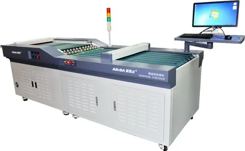
Practical 3D PCB Component Placement Strategies
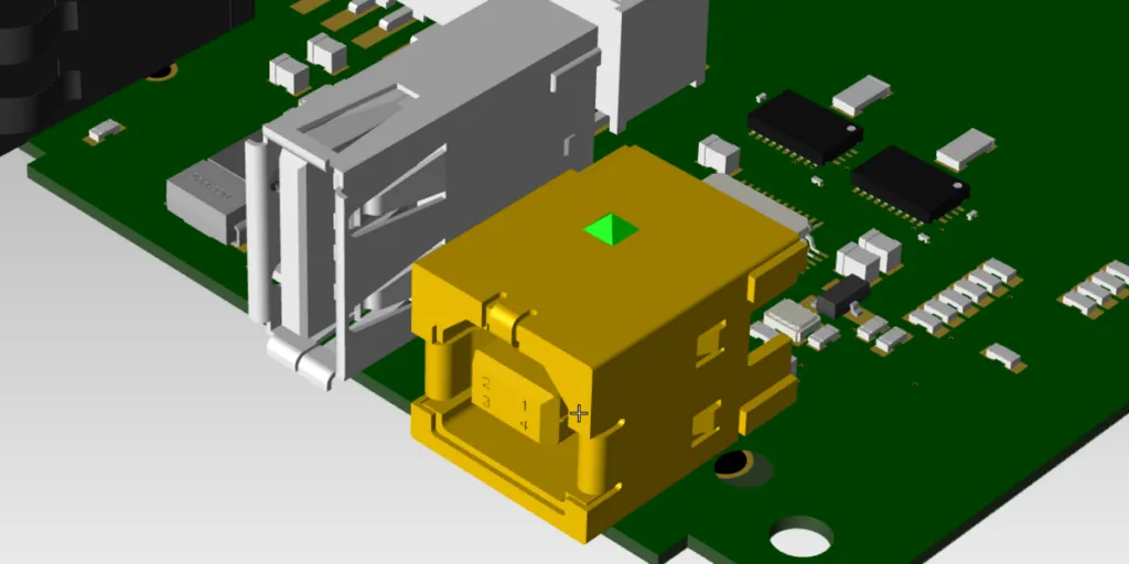
Component placement begins with a thorough review of the overall stackup to identify available vertical real estate and thermal pathways. High-power devices are typically positioned near the outer layers or adjacent to heat-spreading features to facilitate dissipation. Passive components and decoupling capacitors should sit close to active devices yet avoid obstructing vertical via channels needed for power and ground distribution. Orientation of parts with directional sensitivity, such as inductors or connectors, must respect both electrical and mechanical constraints imposed by neighboring layers. These placement decisions form the foundation of reliable 3D PCB design rules that subsequent routing must follow.
Grouping related functions into vertical modules reduces the length of critical nets and simplifies later routing. Designers also reserve clearance zones around stacked components to accommodate manufacturing tolerances and inspection access. Thermal vias placed directly beneath heat-generating devices provide low-resistance paths to inner copper planes or external heat sinks. Balancing component mass across the board area helps control warpage during thermal excursions.
Related Reading: Unlocking Design Freedom: How 3D PCBs are Revolutionizing Electronics Manufacturing
3D PCB Routing Strategies and Design Rules
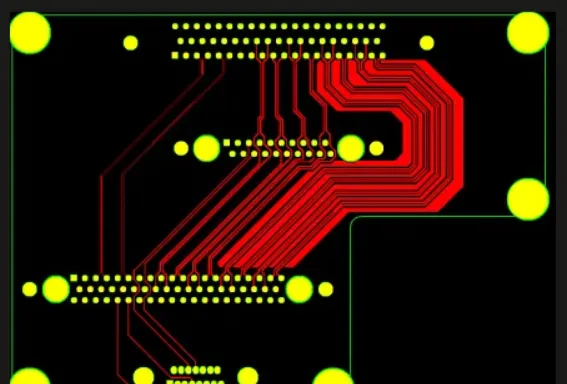
Routing in three dimensions requires coordination between horizontal traces on each layer and vertical interconnects that link them. Via-in-pad or stacked via configurations shorten return paths but demand precise control of plating thickness and fill material to avoid voids. Differential pairs and high-speed signals benefit from controlled impedance routing that accounts for the dielectric properties of all intervening layers. Power distribution networks often employ multiple parallel vias to lower inductance and distribute current evenly across planes. Adherence to these practices supports the acceptance criteria described in IPC-A-600K for printed board quality.
Design rules should specify minimum via diameters, annular ring sizes, and spacing between vertical features to prevent manufacturing defects. Trace widths and clearances may need adjustment based on the cumulative thickness of the stack rather than a single layer. Engineers also define keep-out zones around mechanical mounting holes and edge connectors to preserve structural integrity. Simulation tools help validate that the completed routing meets signal integrity and thermal targets before fabrication.
Related Reading: 3D PCB Printing for Aerospace: A New Dimension in Circuitry
Additional Considerations for Reliable Implementation
Layer-to-layer registration tolerances become tighter in 3D constructions because misalignment affects via continuity and impedance. Designers therefore incorporate fiducial patterns and process compensation factors during artwork generation. Material selection influences both electrical performance and mechanical stability, so stackup documentation should include dielectric constants, glass transition temperatures, and coefficient of thermal expansion values. These parameters guide decisions on via fill materials and surface finishes that maintain reliability through assembly and field use.
Conclusion
Successful 3D PCB projects rest on early application of structured 3D PCB layout guidelines, thoughtful 3D PCB component placement strategies, and disciplined 3D PCB routing strategies. By following established 3D PCB design rules and referencing standards such as those from IPC, engineering teams achieve higher density without sacrificing manufacturability or reliability. Consistent attention to thermal, mechanical, and electrical interactions across all three dimensions produces boards that perform as intended throughout their service life.
FAQs
Q1: What are the primary 3D PCB layout guidelines engineers should follow during initial design?
A1: Engineers begin by defining a balanced stackup that accounts for thermal expansion, copper distribution, and via aspect ratios. Component placement prioritizes short vertical interconnects for critical signals while maintaining adequate spacing for manufacturing tolerances. Routing strategies then focus on controlled impedance paths and robust power distribution through multiple parallel vias. These steps, applied sequentially, reduce the risk of warpage and signal integrity issues in the finished assembly.
Q2: How do 3D PCB component placement strategies differ from conventional two-dimensional approaches?
A2: Placement in 3D designs considers vertical stacking options and thermal pathways through multiple layers in addition to lateral positioning. High-power or heat-sensitive parts are located near outer surfaces or dedicated heat-spreading features. Related functional blocks are grouped vertically to shorten interconnect lengths. This three-dimensional thinking requires simultaneous evaluation of mechanical balance and electrical performance across the entire stack.
Q3: What 3D PCB routing strategies help maintain signal integrity in stacked constructions?
A3: Routing strategies emphasize short, well-defined return paths using stacked or filled vias where appropriate. Differential pairs and high-speed nets receive controlled impedance treatment that incorporates the dielectric properties of all layers. Power and ground planes are connected with sufficient via density to minimize inductance. These practices, combined with appropriate spacing rules, support reliable operation at elevated frequencies.
Q4: Which 3D PCB design rules most directly influence long-term reliability?
A4: Rules governing via aspect ratios, annular ring dimensions, and copper balance across layers have the strongest influence on reliability. Proper clearance around mechanical features and thermal vias beneath heat sources further protect solder joints during temperature cycling. Adherence to these parameters, verified through simulation and prototype evaluation, helps boards withstand environmental stresses over their intended lifespan.





