 ALLPCB


Integrating Bluetooth Low Energy (BLE) on Wearable PCBs
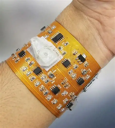
Wearable devices rely on compact electronics to deliver continuous health monitoring, fitness tracking, and connectivity features. Bluetooth Low Energy, commonly known as BLE, has become a preferred wireless technology for these applications because it supports low data rates while maintaining extended battery life. Engineers designing printed circuit boards for wearables must address module integration, antenna performance, and power management from the earliest layout stages. Proper planning ensures reliable communication without compromising the small form factors typical of wristbands, patches, and smart clothing.
Why BLE Integration Matters for Wearable Electronics
BLE enables devices to transmit sensor data such as heart rate, motion, and temperature over distances of several meters while consuming far less energy than classic Bluetooth. This efficiency supports multi-day operation on small lithium-polymer cells, which is essential for user acceptance in medical and consumer wearables. Integration challenges arise because the radio section shares the same board with microcontrollers, sensors, and power management circuits. Successful designs balance signal integrity, thermal considerations, and mechanical constraints imposed by flexible or rigid-flex substrates. Industry standards such as those outlined in IPC-2221 provide foundational guidance for trace widths and spacing that support reliable high-frequency operation.
Technical Principles of BLE Module Integration
A BLE module typically contains the radio transceiver, baseband processor, and protocol stack in a single package that mounts directly onto the PCB. Integration begins with selecting a module footprint that matches the board stack-up and thermal requirements. The module communicates with the host microcontroller through UART, SPI, or I2C interfaces, requiring careful routing to minimize crosstalk with analog sensor lines. Power domains must remain isolated to prevent digital noise from affecting the sensitive receiver front end. Antenna performance depends on the module’s internal or external antenna option, with external designs offering greater flexibility for custom tuning.
Antenna Placement Considerations
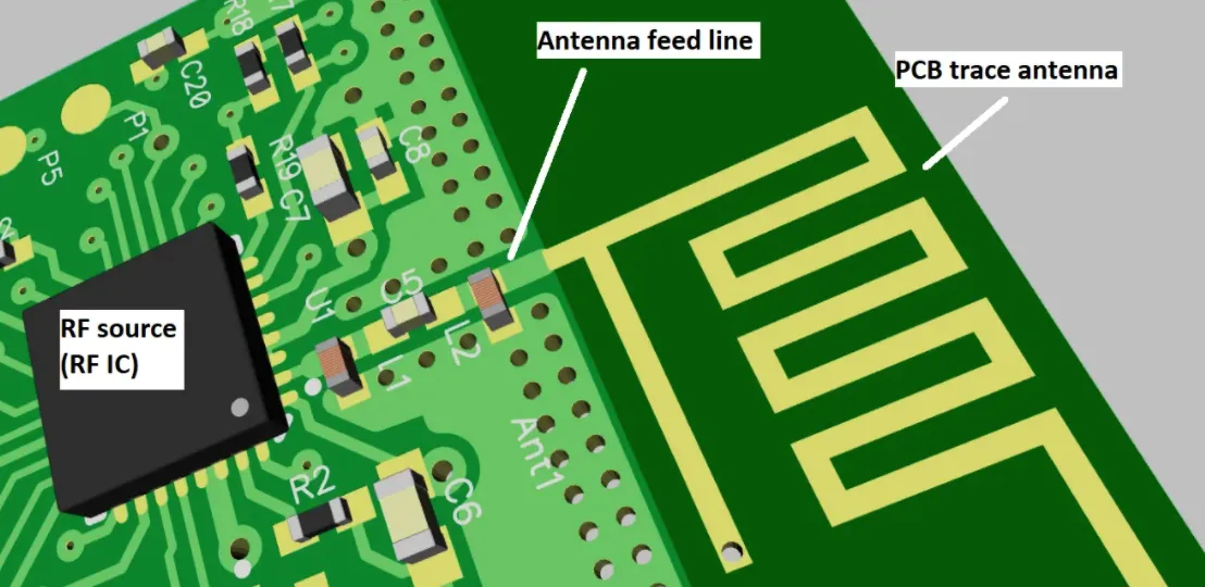
Antenna placement directly influences range, data throughput, and power consumption in BLE systems. The antenna should occupy a clear area on the board edge or corner, free from ground planes, metal shields, or dense component clusters that could detune the radiator. Keep-out zones around the antenna follow manufacturer recommendations and account for the dielectric properties of the enclosure material. Ground stitching vias placed along the perimeter of the RF section help maintain a solid reference plane and reduce radiation leakage into other circuit areas. Engineers often evaluate multiple placement options through simulation before committing to a final layout.
Power Consumption Optimization Techniques
Optimizing power consumption begins with firmware control of BLE connection intervals, advertising duty cycles, and sleep modes. Hardware layout supports these strategies by providing clean power rails with adequate decoupling capacitors placed close to the module supply pins. Separate analog and digital ground returns reduce noise coupling that could force the radio to retransmit packets and increase average current draw. Low-dropout regulators or switched-mode supplies chosen for the RF section must deliver stable voltage under varying load conditions without introducing switching spurs in the 2.4 GHz band. Thermal vias under the module help dissipate heat that would otherwise raise leakage currents in the silicon.
BLE PCB Layout Guidelines
Layout guidelines emphasize controlled impedance for RF traces when an external antenna is used. Microstrip or coplanar waveguide structures maintain 50 ohm characteristic impedance when calculated according to board thickness and copper weight. Sensitive analog traces from sensors route away from the RF section and cross digital lines at right angles where crossings are unavoidable. Component placement clusters the BLE module with its supporting passives while maintaining adequate spacing for rework access. IPC-A-600 acceptance criteria guide visual inspection of solder joints and copper features after assembly to ensure long-term reliability under flexing or temperature cycling typical of wearable use.
Testing BLE Performance on Assembled Boards
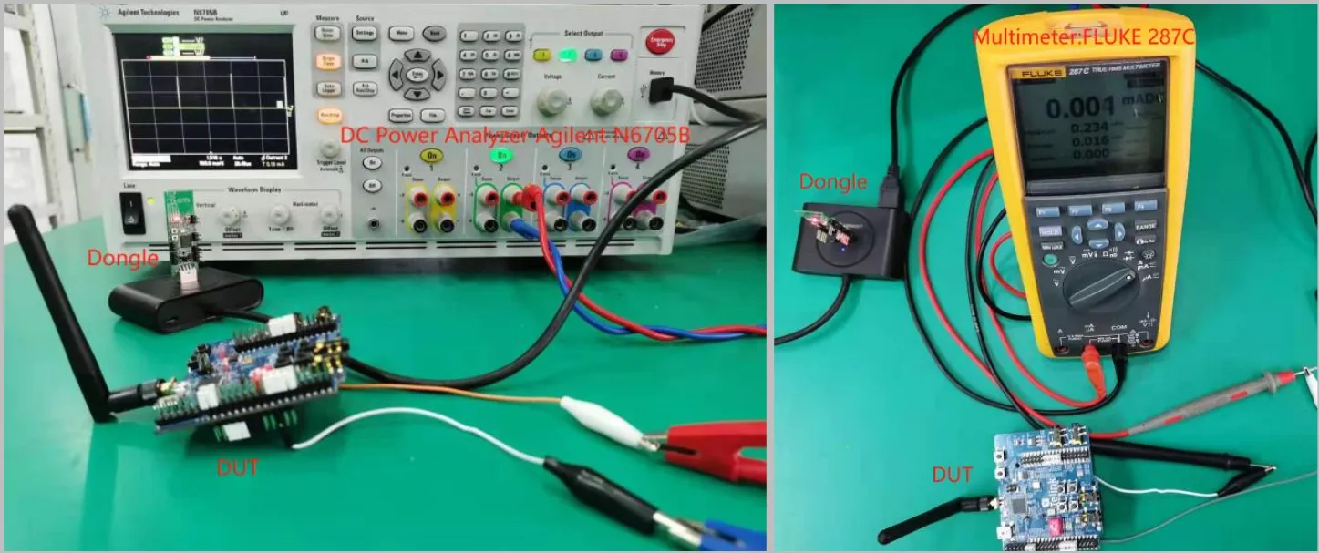
Performance validation includes over-the-air range testing in representative environments, packet error rate measurements, and current consumption profiling across advertising and connected states. Engineers use shielded enclosures or anechoic chambers to isolate the device under test and obtain repeatable results. Antenna efficiency can be verified through return loss measurements with a vector network analyzer before final enclosure integration. Firmware logging of received signal strength indicator values helps correlate layout choices with real-world link quality. Any deviations from expected performance prompt iterative layout adjustments, such as relocating decoupling components or revising ground stitching patterns.
Conclusion
Integrating BLE on wearable PCBs requires coordinated attention to module selection, antenna placement, power architecture, and layout discipline. Following established PCB design practices and performing thorough validation testing produces reliable wireless performance within the tight size and power budgets demanded by wearable applications. Engineers who address these elements early in the design cycle reduce the need for costly board revisions and accelerate time to market.
FAQs
Q1: How does antenna placement affect BLE module integration on wearable PCBs?
A1: Antenna placement determines signal strength and connection stability because nearby metal or dielectric materials can detune the radiator and increase power consumption through retransmissions. Engineers position the antenna at the board edge with adequate keep-out zones and ground stitching to maintain consistent performance across different enclosure materials and user positions.
Q2: What layout practices support power consumption optimization for BLE in wearables?
A2: Clean power distribution, strategic decoupling, and separation of analog and digital grounds minimize noise that would otherwise cause the radio to operate at higher transmit power levels. Proper trace routing and component placement further reduce parasitic losses, allowing the system to spend more time in low-power sleep modes while meeting application throughput requirements.
Q3: Which BLE PCB layout guidelines address high-frequency signal integrity?
A3: Guidelines recommend controlled-impedance traces for RF paths, adequate ground planes, and via stitching to contain electromagnetic fields. These practices, aligned with IPC-2221 recommendations, help maintain signal integrity and reduce interference with other circuits on the compact wearable board.
Q4: How is testing BLE performance typically performed during wearable PCB development?
A4: Testing involves range measurements, packet error rate analysis, and current profiling under various connection scenarios. Results guide layout refinements and confirm that the integrated design meets both wireless and power targets before production release.





