 ALLPCB


What Is PCB Impedance Control and Why It Matters
PCB impedance control refers to the practice of designing conductive traces so their characteristic impedance matches the requirements of the connected circuits. Characteristic impedance depends on trace geometry, the surrounding dielectric materials, and the proximity to reference planes. On maximum PCBs, longer traces amplify the effects of any mismatch, leading to signal reflections that degrade integrity. Industry professionals recognize that uncontrolled impedance can limit operating frequencies and increase bit error rates. Effective control therefore becomes essential for maintaining functionality as board sizes grow.
The relevance of PCB impedance control extends to signal integrity on large PCBs, where propagation delays and crosstalk become more pronounced. Designers must account for these factors early in the layout process to avoid costly revisions later. Consistent impedance supports clean edges and predictable timing across extended distances. Without it, systems may fail to operate at intended speeds or exhibit intermittent faults. This makes impedance management a core consideration in modern board development.
Technical Principles of Trace Impedance Calculation
Trace impedance arises from the interaction between inductance and capacitance per unit length along a conductor. Wider traces lower impedance while narrower traces raise it, assuming other variables remain fixed. Dielectric thickness and the material's relative permittivity further influence the final value. On large PCBs, variations in copper thickness or substrate properties across the panel can introduce inconsistencies that affect overall performance. Engineers therefore calculate impedance using established formulas that incorporate these parameters before finalizing layouts.
Differential pairs require additional attention because their impedance depends on both the individual trace values and the coupling between them. Spacing between the pair members must be controlled precisely to achieve the target differential impedance. Reference plane continuity also plays a critical role, as discontinuities create impedance variations that reflect signals. In maximum PCBs, maintaining plane integrity across large areas demands careful planning of vias and cutouts. These principles guide the structured approach to achieving controlled impedance PCBs.
Practical Solutions and Best Practices for Impedance Matching Techniques
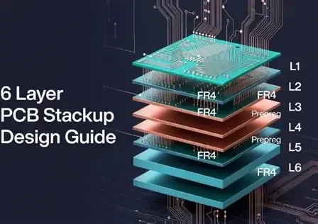
Designers begin by defining target impedance values based on the specific interface standards used in the system. Stackup planning follows, with dielectric thicknesses and copper weights selected to support the required trace geometries. Impedance matching techniques include adjusting trace widths, using serpentine routing for length equalization, and incorporating termination resistors where appropriate. Simulation tools verify that the intended values will be achieved after fabrication tolerances are considered. This proactive method reduces the likelihood of post-production adjustments.
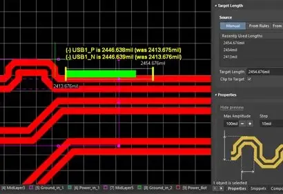
During layout, maintaining consistent reference planes beneath critical traces minimizes impedance deviations. Ground pours and stitching vias help preserve return paths on large boards. When routing across multiple layers, transitions must preserve impedance continuity to avoid reflections. Regular review of trace geometries against calculated targets ensures compliance throughout the design. These steps collectively support reliable signal integrity on large PCBs.
Conclusion
Effective PCB impedance control directly influences the reliability of signal transmission on maximum PCBs. By applying structured calculations and matching techniques, engineers achieve the consistency required for high-performance operation. Attention to stackup, geometry, and reference integrity throughout the process supports predictable results. These practices remain fundamental as board dimensions and signal speeds continue to increase.
FAQs
Q1: What factors determine trace impedance in PCB impedance control?
A1: Trace width, copper thickness, dielectric constant, and height above the reference plane are primary factors. On large PCBs, maintaining uniformity across extended areas requires careful material selection and layout discipline. Consistent application of these parameters enables predictable signal behavior and supports signal integrity on large PCBs.
Q2: How do impedance matching techniques improve performance on maximum PCBs?
A2: Impedance matching techniques align trace characteristics with driver and receiver requirements, reducing reflections and preserving signal edges. Length tuning and proper termination further minimize timing skew across longer paths. These methods help sustain reliable operation as board sizes increase.
Q3: Why is trace impedance calculation important for controlled impedance PCBs?
A3: Trace impedance calculation allows designers to select geometries that achieve target values before fabrication. It accounts for manufacturing tolerances and material variations that affect final results. Accurate calculation supports the development of controlled impedance PCBs that meet electrical specifications.
Q4: What role does stackup play in signal integrity on large PCBs?
A4: Stackup defines the dielectric thicknesses and plane arrangements that determine impedance. Proper planning ensures reference continuity and consistent electrical characteristics across extended traces. This foundation is essential for maintaining signal integrity on large PCBs.
References
IPC-2221B — Generic Standard on Printed Board Design. IPC, 2012
IPC-6012E — Qualification and Performance Specification for Rigid Printed Boards. IPC, 2017
IPC-A-600K — Acceptability of Printed Boards. IPC, 2020





