 ALLPCB


Heavy copper PCBs support demanding electrical and thermal loads in high-power designs. Increasing copper thickness on inner layers becomes necessary when standard constructions cannot meet current-carrying requirements or thermal constraints. Engineers evaluate this option during the design phase for applications involving motors, power converters, and systems operating in elevated temperatures or harsh conditions. The decision balances performance gains against manufacturing complexity and cost. Proper planning ensures reliable operation without exceeding material or process limits.
What Is Heavy Copper PCB and Why Inner Layer Thickness Matters
Heavy copper PCB refers to constructions where copper weight exceeds three ounces per square foot on one or more layers. Inner layer copper thickness directly influences current handling capacity and heat spreading within a multilayer stack-up. In high-power PCB design, inner layers often carry the bulk of the current in complex routing schemes. Extreme environment electronics place additional demands on these layers because external cooling may be limited. Thick copper benefits include reduced voltage drop and improved mechanical stability under thermal cycling. Designers specify inner layer copper when trace widths alone cannot satisfy ampacity needs without violating board size constraints.
Technical Principles of Inner Layer Current Handling
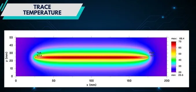
Current flow through copper traces generates heat according to resistive losses. Inner layers dissipate this heat primarily through conduction to adjacent planes and outer surfaces. Increasing copper thickness lowers resistance and allows wider effective current paths without enlarging trace geometry. Thermal expansion differences between copper and dielectric materials can induce stress during temperature excursions. IPC-6012E outlines qualification requirements that address conductor integrity under such conditions. In extreme environment electronics, vibration and shock further test the adhesion between thick copper and laminate. Proper thickness selection maintains acceptable temperature rise while preserving dielectric integrity across the operating range.
Manufacturing processes for inner layers involve sequential lamination and etching steps. Thicker copper requires controlled etch factors to maintain trace definition and avoid undercutting. Heat transfer improves as copper mass increases, yet excessive thickness can affect impedance control in high-speed sections. Engineers model these interactions using finite element analysis to predict current distribution and hot-spot formation. IPC-A-600K provides visual and dimensional acceptance criteria that apply equally to standard and heavy copper constructions.
Practical Solutions and Best Practices for High-Power PCB Design
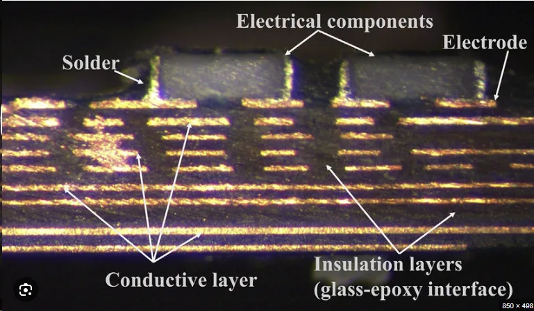
Designers begin by calculating required copper weight using established current-carrying guidelines for the target temperature rise. When inner layer traces must handle sustained loads above typical limits, increasing thickness from one or two ounces to four or six ounces provides headroom. Layer stack-up planning places heavy copper planes adjacent to heat-generating components for efficient spreading. Thermal vias connect inner copper to outer surfaces or heat sinks when direct conduction proves insufficient.
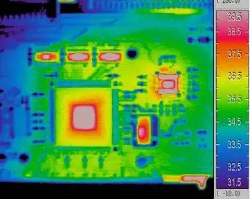
Fabrication reviews confirm that selected copper weights remain compatible with chosen dielectrics and lamination cycles. Etch compensation and plating uniformity receive attention to avoid defects that could compromise reliability. In high-power PCB design, simulation of both electrical and thermal performance precedes layout finalization. Procurement teams verify that the chosen construction aligns with available manufacturing capabilities for the required board size and layer count.
Manufacturing and Quality Considerations
Inner layer processing demands tighter control of etch rates and surface preparation when copper exceeds standard weights. Registration accuracy between layers becomes critical to maintain via alignment and prevent shorts or opens. Quality control procedures include microsection analysis to verify copper thickness and adhesion after lamination. IPC-A-600K acceptance criteria guide inspectors in evaluating conductor width, spacing, and surface condition on heavy copper layers. These steps ensure the finished board meets performance expectations in extreme environment electronics.
Conclusion
Increasing inner layer copper thickness addresses current handling and thermal management challenges in high-power PCB design. The approach delivers measurable benefits when standard constructions fall short, provided engineers account for manufacturing constraints and material interactions. Structured evaluation using industry guidelines supports reliable outcomes across demanding applications.
FAQs
Q1: When should designers consider heavy copper PCB for inner layers?
A1: Designers evaluate heavy copper PCB when calculated current requirements exceed the capacity of standard one- or two-ounce copper at acceptable temperature rise. Inner layer current handling improves with added thickness, supporting compact layouts in high-power applications. Evaluation includes stack-up review and thermal modeling before committing to fabrication.
Q2: What benefits does thick copper provide in extreme environment electronics?
A2: Thick copper benefits include lower resistive losses and enhanced heat spreading, which help maintain component temperatures within limits during continuous operation. Inner layer current handling capacity increases, reducing the need for excessively wide traces. These characteristics support stable performance under elevated temperatures and mechanical stress.
Q3: How does inner layer copper thickness affect high-power PCB design?
A3: Inner layer copper thickness directly determines the maximum sustainable current before excessive heating occurs. Designers adjust thickness to balance electrical performance, thermal dissipation, and impedance requirements. The resulting stack-up influences overall board reliability in high-power PCB design projects.
Q4: Are there manufacturing limits when specifying heavy copper on inner layers?
A4: Manufacturing limits arise from etch control, lamination pressure, and registration accuracy as copper weight increases. Quality standards such as those in IPC-6012E guide acceptable parameters. Early collaboration with fabricators confirms feasibility for the chosen thickness and layer count.
IPC-6012E — Qualification and Performance Specification for Rigid Printed Boards. IPC, 2017
IPC-A-600K — Acceptability of Printed Boards. IPC, 2020
IPC-2152 — Standard for Determining Current Carrying Capacity in Printed Board Design. IPC, 2009





