 ALLPCB


Introduction
Fiducial marks serve as critical reference points that guide automated equipment during the stencil alignment process in printed circuit board assembly. In high-density designs, where component pitches shrink below 0.5 millimeters, even minor misalignment can lead to solder paste defects and reduced yield. Engineers rely on these marks to achieve the stencil alignment accuracy required for consistent paste deposition across fine-pitch pads. Proper fiducial mark design and fiducial mark placement therefore form foundational elements of modern surface-mount technology workflows. The following sections examine the principles, best practices, and standards that support reliable alignment outcomes.
What Fiducial Marks Are and Why They Matter
A fiducial mark consists of a precisely defined copper feature, typically circular, that remains exposed on the outer layers of a printed circuit board. These marks enable vision systems in stencil printers and pick-and-place machines to locate the board coordinate system with sub-millimeter precision. In high-density assembly, the absence of well-defined fiducials increases the risk of paste bridging or insufficient coverage on small pads. Industry standards such as IPC-7525 guide the recommended dimensions and tolerances for stencil-related alignment features. Effective use of fiducial marks therefore directly influences both manufacturing throughput and long-term product reliability.
Technical Principles of Alignment
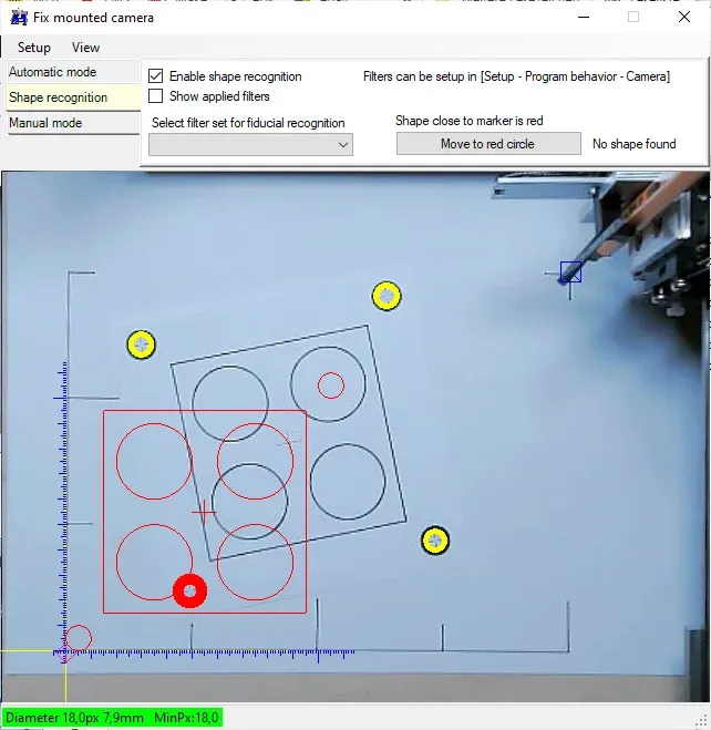
Stencil alignment begins when the printer camera identifies the centers of the fiducial marks and calculates the offset between the board and the stencil aperture pattern. The system then applies X, Y, and theta corrections before lowering the stencil into contact with the board surface. Fiducial mark size typically ranges from 1.0 to 3.0 millimeters in diameter, with the exact value chosen to balance recognition reliability against available board real estate. Copper thickness and surface finish affect contrast under the camera lighting, so designers often specify a bare-copper or matte finish around the mark. Thermal expansion of the board material during reflow can shift fiducial positions slightly, requiring the alignment algorithm to incorporate compensation factors derived from material coefficients.
Related Reading: SMT Stencil Capabilities: Panel Fiducials positioning points for Automated stencil machine
Fiducial Mark Design Considerations
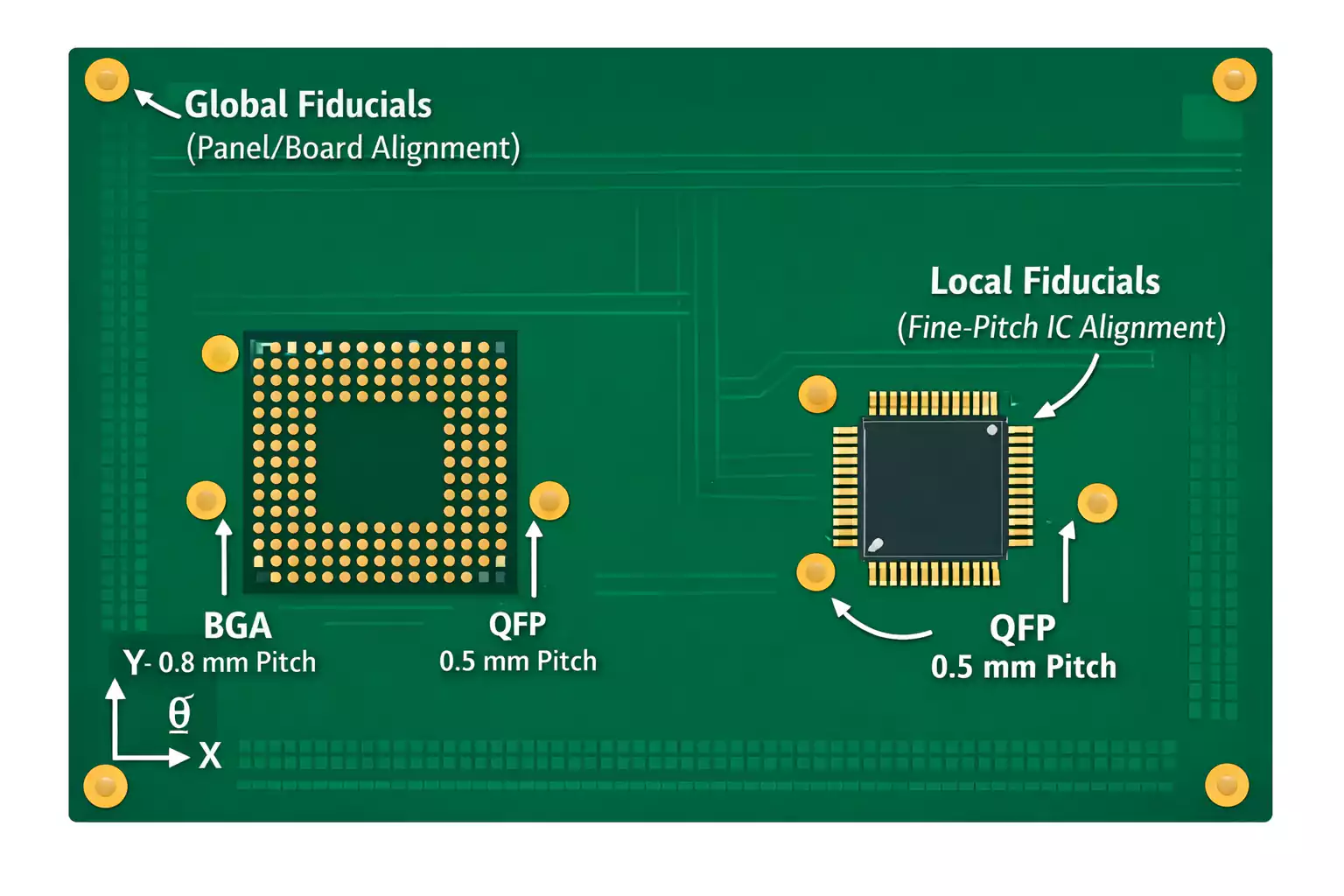
Engineers determine fiducial mark design by evaluating board size, component density, and the expected variation in material properties. A minimum clearance zone of 2.0 millimeters around each mark prevents solder mask encroachment that could degrade optical recognition. Placement of at least three non-collinear fiducials, typically at the corners of the board, allows the vision system to compute both translation and rotation errors. When board warpage exceeds 0.75 percent, additional fiducials near high-density regions improve local alignment accuracy. Consistent pad geometry across all marks ensures repeatable centroid calculation by the imaging software.
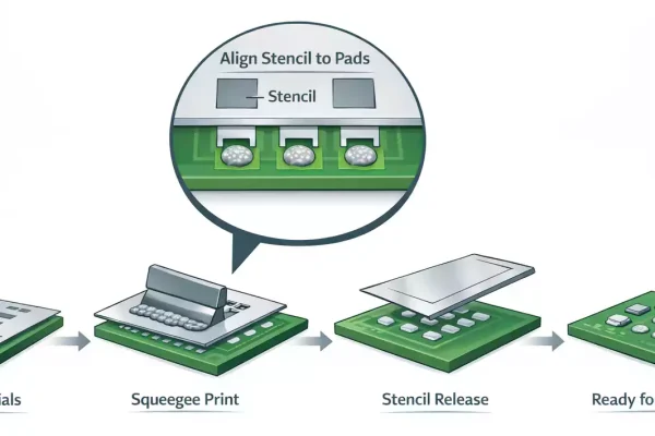
Stencil Alignment Process and Accuracy Requirements
The stencil alignment process follows a sequence of image capture, feature extraction, and mechanical adjustment. First, the printer locates the fiducials on the bare board. Next, it compares their measured positions against the programmed coordinates stored in the machine recipe. Any deviation triggers servo corrections that bring the stencil apertures into registration with the copper pads. Target stencil alignment accuracy for high-density assemblies is commonly held to plus or minus 25 micrometers to maintain adequate paste volume on 0.4-millimeter pitch components. Regular verification of camera calibration and lighting intensity supports sustained performance over production runs.
Related Reading: Stencil Alignment Techniques: The Role of Material Stability in Accurate Paste Deposition
Best Practices for Fiducial Mark Placement
Design teams locate fiducials away from board edges by at least 5.0 millimeters to avoid fixturing interference. Symmetric placement relative to the board center minimizes the impact of asymmetric shrinkage during lamination. When panels contain multiple boards, each individual board should carry its own set of fiducials so that the printer can align to every unit independently. Documentation of fiducial coordinates in the Gerber files must match the physical layout exactly, including layer-specific offsets. Periodic audits of placement accuracy during first-article inspection confirm that manufacturing tolerances remain within acceptable limits.
Troubleshooting Common Alignment Issues
When stencil alignment accuracy falls outside specification, the first diagnostic step is to inspect fiducial contrast under the actual printer lighting. Oxidation or residue on the copper surface can reduce edge definition and cause centroid calculation errors. Adjusting camera gain or switching to a different illumination wavelength often restores reliable detection. If mechanical drift appears after several hundred cycles, verification of stencil frame flatness and vacuum table condition becomes necessary. Consistent monitoring of these factors prevents recurring defects in high-volume production.
Conclusion
Fiducial mark design and fiducial mark placement remain essential controls for achieving the stencil alignment accuracy demanded by high-density printed circuit board assembly. Structured attention to mark size, clearance zones, and non-collinear positioning enables vision systems to deliver repeatable results. Adherence to established industry standards such as IPC-7525 and IPC-A-610 further supports consistent process capability across different manufacturing environments. By integrating these practices into the design phase, engineering teams reduce defect rates and improve overall assembly yield.
FAQs
Q1: How does fiducial mark size influence stencil alignment accuracy?
A1: Fiducial mark size directly affects the precision with which vision systems calculate the board coordinate reference. Larger marks improve edge detection under varying lighting conditions, while excessively large marks consume valuable board space. Industry guidelines recommend diameters between 1.0 and 3.0 millimeters for most high-density applications. Proper sizing therefore balances recognition reliability with layout constraints.
Q2: What factors determine optimal fiducial mark placement on complex boards?
A2: Optimal fiducial mark placement accounts for board dimensions, component density, and expected thermal behavior during processing. Engineers position marks at three or more non-collinear locations, typically near the corners, to capture both translation and rotation errors. Adequate clearance from edges and solder mask ensures unobstructed camera views. These choices collectively support the stencil alignment process across production volumes.
Q3: Why is the stencil alignment process critical for high-density assembly?
A3: The stencil alignment process translates fiducial data into mechanical corrections that register paste deposits with copper pads. In high-density layouts, even small offsets produce insufficient or excessive solder volumes that compromise joint integrity. Maintaining alignment within plus or minus 25 micrometers preserves yield and reduces rework. Consistent execution of this process therefore underpins overall manufacturing quality.
Q4: How do industry standards guide fiducial mark design practices?
A4: Standards such as IPC-7525 and IPC-A-610 define acceptable geometries, tolerances, and inspection criteria for fiducial features used in stencil alignment. These documents specify minimum clearances, surface finish recommendations, and verification methods that promote repeatable machine performance. Following the guidance reduces variability between design intent and fabricated boards. Compliance therefore supports both process capability and long-term reliability.
References
IPC-7525B — Stencil Design Guidelines. IPC, 2018
IPC-A-610H — Acceptability of Electronic Assemblies. IPC, 2020


