 ALLPCB


Introduction
Replacing tiny components on printed circuit boards has become a common challenge in DIY electronics repair, especially as devices pack more micro-components like 01005 resistors or fine-pitch QFNs. Traditional methods such as hot air rework or desoldering braid often risk damaging delicate pads or nearby traces due to their lack of precision. Laser drilling electronics repair offers a targeted solution by using focused laser energy to ablate solder, residue, or excess solder mask without affecting surrounding areas. This technique prepares pads cleanly for laser soldering prep, making it ideal for hobbyists tackling smartphone boards or wearable tech. As electronics shrink, mastering this method enhances repair success rates and preserves board integrity. Hobbyists can achieve professional results at home with affordable laser setups.
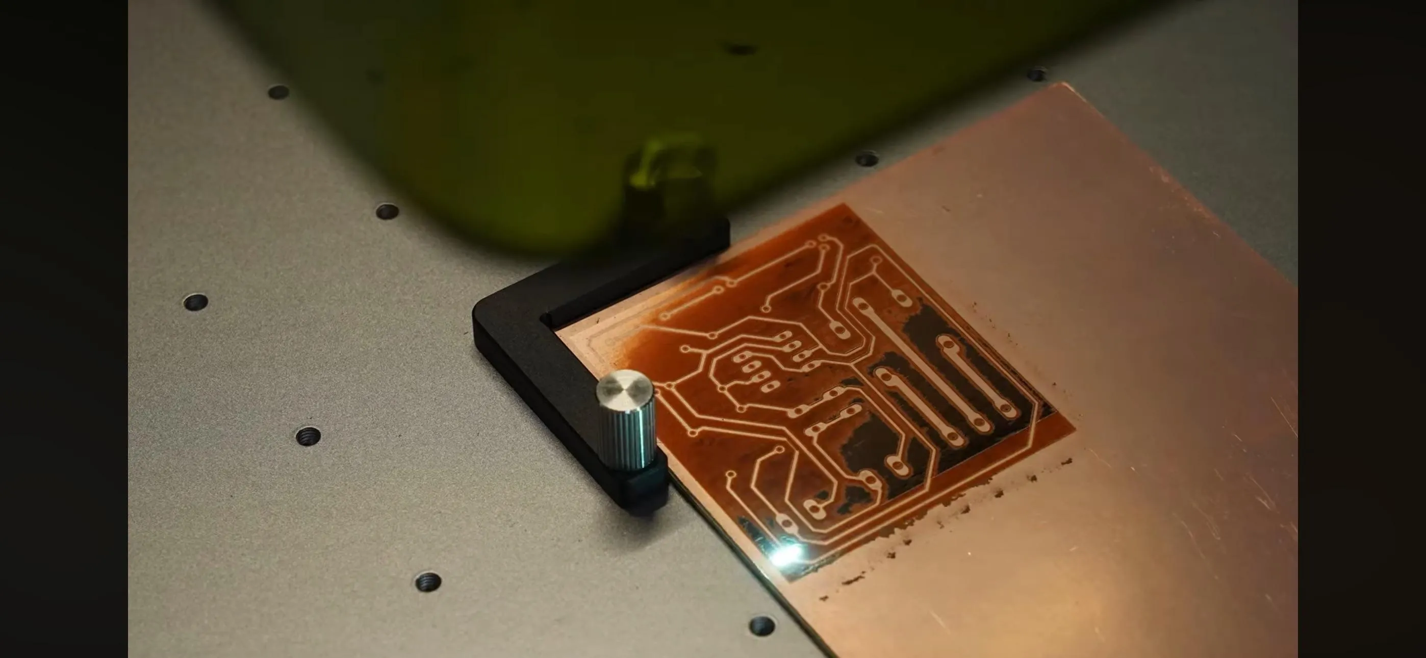
What Is Laser Drilling in Electronics Repair and Why It Matters
Laser drilling in electronics repair involves directing a pulsed laser beam to vaporize specific materials on a PCB surface, creating clean access for component replacement. Unlike mechanical drilling, which generates heat and debris, laser drilling provides micron-level precision essential for replacing micro-components under 0.4mm. This process matters because modern PCBs feature densely packed tiny SMDs where pads are often bridged by old solder or covered by damaged mask, complicating rework. For DIY electronics repair enthusiasts, it reduces the trial-and-error of scraping or chemical cleaners that can lift traces. Industry standards like IPC-7711/7721 emphasize controlled material removal during rework to maintain assembly reliability. Ultimately, laser drilling bridges the gap between hobbyist tools and factory precision.
In high-density boards from consumer gadgets, micro-components fail due to thermal stress or manufacturing defects, demanding exact pad preparation. Without proper cleaning, new solder joints form voids or bridges, leading to intermittent failures. Laser drilling electronics repair minimizes these issues by selectively removing contaminants, aligning with J-STD-001 requirements for solder joint quality. Hobbyists benefit from shorter repair times and higher success on multilayer boards. This method also supports sustainability by extending device lifespans through effective repairs.
Technical Principles of Laser Drilling for PCB Rework
Lasers for electronics repair typically operate in the UV, diode, or fiber wavelength range, where energy is absorbed by copper, solder, or polymers without deep penetration into the substrate. Pulsed operation delivers short bursts to ablate material through vaporization, avoiding conductive heat transfer that warps FR-4 or delaminates layers. The spot size, often under 50 microns, allows pinpoint targeting of pads for replacing micro-components. Beam parameters like pulse duration and repetition rate control depth, preventing damage to inner traces. Reflection from copper requires careful focus adjustment to ensure efficient energy coupling.
Material interaction varies: solder alloys melt and eject rapidly, while epoxy-based solder mask carbonizes and flakes off cleanly. For laser soldering prep, the process exposes fresh copper oxide-free, promoting strong intermetallic bonds. Adherence to IPC-7711/7721 guidelines ensures the ablated area meets cleanliness criteria before new component placement. Thermal management is key, as excessive pulses raise local temperatures, potentially reflowing adjacent joints. Hobbyists must calibrate power based on board thickness to stay within safe limits.
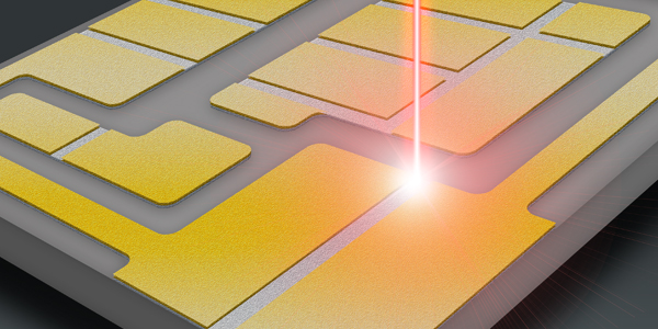
Practical Solutions and Best Practices for DIY Laser Drilling
Start with safety gear including laser safety goggles matched to your wavelength, ventilation for fumes, and a fire-suppressant nearby, as ablation produces particulates and potential ignitions. Secure the PCB in a fixture to prevent movement during laser drilling electronics repair. Identify target pads using magnification; scan the board first to map micro-component sites. Set laser to low power initially, around 1-5W for diode types, and test on scrap material matching your PCB's composition.
Position the laser head perpendicular to the pad surface for uniform ablation. Pulse briefly over the old solder or mask, observing smoke plume as indicator of material removal. Wipe residue with isopropyl alcohol between passes to inspect progress; aim for shiny copper exposure without pitting. For replacing micro-components, drill out bridges first, then feather edges for smooth solder flow. Follow with flux application to activate the pad for laser soldering prep.
Incorporate airflow to cool the board, preventing heat soak into vias. Verify pad flatness post-drilling to ensure reliable SMD seating. Practice on donor boards builds confidence in power settings. Document settings for repeatability across similar repairs.
Troubleshooting Common Issues in Laser Drilling Repair
Over-ablation often stems from high pulse energy, eroding copper pads; reduce power and increase passes for control. If the laser skips reflective solder, apply matte flux beforehand to enhance absorption. Board charring signals poor focus or wrong wavelength; CO2 lasers suit mask removal, while fiber excels on metals. Stuck residue after drilling requires ultrasonic cleaning as a follow-up.
For multilayer boards, monitor for interlayer delamination by tapping post-repair; if detected, halt and bake per J-STD-001 preheat specs. Uneven pad cleaning leads to tombstoning in reflow; re-drill selectively. Component misalignment during placement post-drilling? Use fiducials or tack solder one corner first.
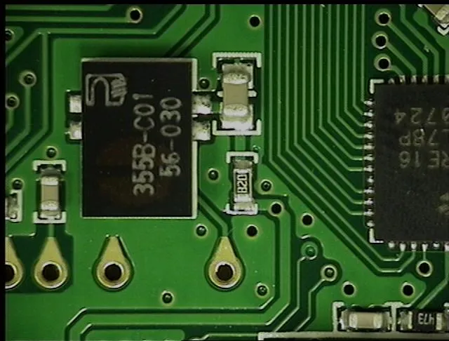
Case in point: A hobbyist repairing a smartwatch PCB faced bridged 0201 caps. Laser drilling cleared joints in seconds without trace lifts, enabling flawless replacement. Key was iterative low-power passes.
Conclusion
Laser drilling electronics repair revolutionizes DIY electronics repair by enabling precise pad preparation for replacing micro-components. From ablation principles to hands-on best practices, this method delivers clean surfaces ready for laser soldering prep. Adhering to standards like IPC-7711/7721 ensures durable results comparable to professional rework. Hobbyists gain efficiency and confidence tackling dense boards. Experiment safely, refine techniques, and extend the life of your gadgets.
FAQs
Q1: What equipment do I need for laser drilling electronics repair at home?
A1: For DIY electronics repair, a diode or fiber laser module with 5-20W power, adjustable focus, and PCB fixture suffices. Pair with safety goggles, magnifier, and flux. Start with scrap boards to dial in settings for replacing micro-components. This setup handles most hobbyist tasks without industrial costs.
Q2: How does laser drilling improve replacing micro-components?
A2: Laser drilling electronics repair removes solder and mask precisely, avoiding mechanical damage to tiny pads. It prepares flat, oxide-free surfaces for better solder wetting during laser soldering prep. Compared to braid, it cuts time and preserves traces on dense boards. Follow IPC-7711/7721 for quality joints.
Q3: Is laser drilling safe for DIY electronics repair on multilayer PCBs?
A3: Yes, with precautions: use pulsed low-power modes to limit heat, ventilate fumes, and monitor temperatures. It suits hobbyists replacing micro-components without delaminating layers. Test on singles first. J-STD-001 guides post-repair inspection for reliability.
Q4: Can laser drilling fix solder bridges on fine-pitch ICs?
A4: Absolutely, targeted ablation clears bridges in laser drilling electronics repair, ideal for QFN or BGA edges. Feather the pad edges post-drill for reflow. Avoid over-pulsing to prevent undercuts. Enhances success in DIY electronics repair.
References
IPC-7711/7721 — Rework of Electronic Assemblies. IPC
J-STD-001 — Requirements for Soldered Electrical and Electronic Assemblies. IPC
IPC-A-610 — Acceptability of Electronic Assemblies. IPC





