 ALLPCB


What Is Solder Mask Thickness and Why It Matters
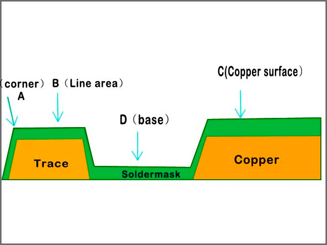
Solder mask is a protective polymer coating applied over copper traces and planes on a printed circuit board. Its thickness refers to the cured height of this coating above the copper surface, typically measured in the areas between traces as well as over the traces themselves. This dimension directly influences several manufacturing steps, including exposure, development, and thermal curing. In design for manufacturability, thickness affects how well the mask prevents solder bridging during reflow and protects against environmental contaminants over the product lifetime. Procurement and engineering teams review these values to align board designs with available fabrication processes and assembly equipment capabilities.
Technical Principles and Mechanisms
The application process begins with liquid or dry-film solder mask materials that are coated or laminated onto the board surface. During exposure and development, the material in non-pad areas remains while openings are created for component terminations. Thickness influences the depth of these openings and the resulting sidewall profile, which in turn affects solder paste release and wetting behavior. Thicker coatings can improve insulation between adjacent conductors but may increase the risk of incomplete curing or trapped volatiles if process parameters are not adjusted accordingly. Thermal expansion mismatch between the mask and substrate materials becomes more pronounced with greater thickness, potentially contributing to localized stress during temperature cycling.
Adhesion strength depends on surface preparation of the copper and the chemistry of the mask formulation. Variations in thickness across a panel can arise from coating method, panel topography, and curing uniformity. These variations are evaluated against acceptability criteria that consider both functional performance and cosmetic appearance. Standards such as IPC-6012E establish qualification requirements that include evaluation of coating integrity under environmental stress.
Practical Solutions and Best Practices
Designers begin by consulting fabrication notes and capability documents from their chosen manufacturing partner. Typical practice calls for specifying a nominal thickness range rather than a single value, allowing the fabricator flexibility while maintaining functional performance. Clearances around pads and traces are set to accommodate the mask thickness and its associated tolerances, preventing the mask from encroaching on solderable areas. When fine-pitch components are present, thinner mask layers in those regions can improve paste release, while thicker layers elsewhere enhance protection.
Review of the stack-up early in the design cycle helps identify areas where copper thickness or trace density may influence final mask height. Simulation of thermal profiles during assembly can highlight potential issues with mask cracking or delamination. Documentation should include both minimum and maximum thickness values along with measurement locations, typically expressed relative to the copper surface. Collaboration between layout and process engineering teams reduces the likelihood of last-minute changes that affect yield.
Troubleshooting and Quality Considerations
Common issues related to solder mask thickness include insufficient coverage leading to exposed copper, excessive thickness causing poor solder joint formation, and uneven application resulting in cosmetic or functional defects. Inspection under magnification or using automated optical systems verifies that openings meet dimensional requirements and that the mask surface remains free of pinholes or bubbles. When defects appear, root-cause analysis often traces back to coating parameters, exposure energy, or post-cure handling.
Standards such as IPC-A-600K provide visual and dimensional acceptance criteria that help teams classify anomalies consistently. Process adjustments may involve changes to coating speed, viscosity, or curing temperature profiles. In high-reliability applications, additional testing such as thermal shock or humidity exposure confirms that the chosen thickness maintains performance throughout the expected service life. Documentation of these evaluations supports traceability and continuous improvement.
Conclusion
Optimizing solder mask thickness requires attention to material behavior, process capabilities, and end-use requirements. Early specification of appropriate ranges, combined with clear communication of tolerances and measurement methods, supports both manufacturability and long-term reliability. Regular review against established industry criteria helps maintain consistency across production lots. Design teams that integrate these considerations achieve higher first-pass yields and fewer field issues.
FAQs
Q1: What role does solder mask thickness play in DFM for printed circuit boards?
A1: Solder mask thickness influences several fabrication and assembly steps, including pad definition, solder paste release, and insulation between conductors. Specifying an appropriate range early in the design process helps align the layout with manufacturing capabilities and reduces the chance of defects such as bridging or exposed copper. Consistent thickness also supports reliable performance under thermal and environmental stress.
Q2: How do design rules address solder mask thickness variations?
A2: Design rules typically define minimum and maximum thickness values along with required clearances around pads and traces. These rules account for process tolerances and ensure that the mask does not interfere with soldering while still providing adequate coverage. Reviewing these parameters against fabricator capabilities allows adjustments before layout completion.
Q3: Why is solder mask thickness important for PCB assembly reliability?
A3: Thickness affects the profile of mask openings and the ability of solder to wet properly during reflow. Excessively thick mask in fine-pitch areas can trap paste or create high edges that hinder component placement. Proper control of thickness therefore contributes to consistent joint formation and reduced risk of opens or shorts after assembly.
Q4: What standards guide evaluation of solder mask thickness?
A4: Industry standards such as those from IPC provide qualification and acceptability criteria for coating thickness, adhesion, and overall integrity. These documents help teams establish consistent measurement methods and acceptance limits that apply across different board constructions and end-use environments.


