 ALLPCB


Introduction
For electronic hobbyists diving into PCB panel size DIY projects, understanding panelization can transform frustrating single-board etching sessions into efficient production runs. Imagine etching multiple identical circuits on one large sheet, saving time and materials while mimicking professional small batch PCB assembly workflows. This guide breaks down PCB panel size essentials, tailored for beginners who etch at home or order small quantities. Whether you are tackling beginner PCB projects panel guidance or exploring home etching panelization, getting the size right ensures better yield and lower costs. Panelization groups several boards into a single panel, optimized for your setup or fabricator's equipment. By the end, you will grasp simple PCB panel methods and affordable panel size options to elevate your hobby projects.
What Is PCB Panel Size and Why It Matters for Hobbyists
PCB panel size refers to the overall dimensions of an array where multiple individual printed circuit boards are arranged and connected, ready for fabrication and depanelization. In hobbyist contexts, this means deciding how many boards fit onto a sheet that suits your etching tank, drill press, or mail-order service. Standard panels in industry might span larger formats, but for DIY, sizes range from postcard dimensions up to 12 by 18 inches, depending on your tools. The key benefit lies in economy: fabricating one panel instead of individuals cuts handling time and waste, crucial for small batch PCB assembly.
Panelization matters because mismatched sizes lead to poor material use or processing failures. For home etching panelization, a panel too large bows under its weight, causing uneven exposure. Hobbyists often overlook how panel size affects registration accuracy during alignment. Proper sizing aligns with basic tolerances in standards like IPC-A-600, ensuring acceptability in visual and dimensional checks. Ultimately, smart panel choices make affordable panel size options accessible, boosting project success rates.
Key Factors Influencing PCB Panel Size Choices
Several engineering factors dictate ideal PCB panel size DIY configurations. Board count depends on individual PCB dimensions, spacing for v-scoring or tabs, and fiducials for alignment. Material thickness plays a role; thinner FR-4 warps more in larger panels, risking misalignment during soldering. Hobbyists must balance density against stability, aiming for 70 to 90 percent panel utilization without overcrowding.
Aspect ratio influences handling and cutting. Square or near-square panels, like 8 by 10 inches, etch evenly in home baths due to uniform chemical flow. Rectangular ones suit elongated boards but demand robust frames to prevent sagging. Environmental controls, such as room temperature fluctuations, amplify warpage in oversized panels, per guidelines in IPC-6012E for rigid board performance.
Tool constraints further shape decisions. Home drill bits handle smaller panels better, avoiding bit wander on expansive sheets. For small batch PCB assembly, fabricators prefer panels fitting their conveyor systems, often under 20 by 24 inches. Electrical testing probes access inner boards more easily on compact arrays. Considering these ensures simple PCB panel methods yield reliable results.
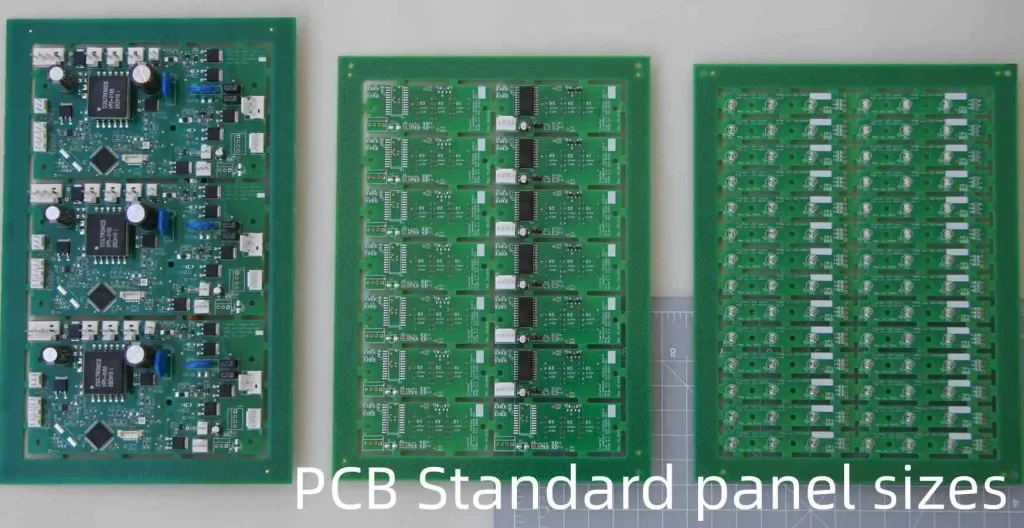
Common PCB Panel Sizes for Hobbyists
Hobbyists favor practical sizes starting small for experimentation. A 4 by 6 inch panel accommodates four to six tiny boards, perfect for beginner PCB projects panel guidance. This scale fits standard photoresist sheets from suppliers, easing home etching panelization. Stepping up, 6 by 9 inches supports medium prototypes, balancing cost and output.
Larger affordable panel size options, such as 10 by 12 inches, maximize small batch PCB assembly efficiency. These fit most desktop routers for depanelization and align with common carrier sheets. Ultra-small 100 by 100 mm panels suit laser etchers, minimizing chemical use. Avoid extremes; panels over 18 inches challenge hobbyist flatbeds.
Customization thrives in DIY. Calculate by dividing sheet stock dimensions by board footprint, adding 5 to 10 mm rails. Test fits virtually first to optimize. Such approaches make panelization straightforward.
- 4 x 6 inches: 4-8 small boards - Best for quick prototypes, home etching.
- 6 x 9 inches: 6-12 medium boards - Best for beginner testing runs.
- 10 x 12 inches: 10-20 boards - Best for small batch assembly.
- 12 x 18 inches: 20+ boards - Best for advanced hobby production.
Simple PCB Panel Methods for Home and Small Batch Use
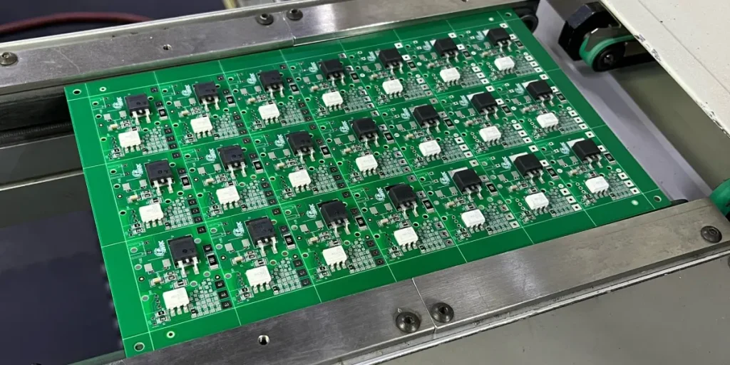
Home etching panelization starts with layout software arranging boards in a grid. Use 1.6 mm spacing between units for v-grooves, ensuring clean depanelization with a pizza cutter or saw. Print the panelized gerber on transparency film for UV exposure. Develop and etch as one unit, then separate. This method scales for affordable panel size options under 10 inches square.
For small batch PCB assembly, tab routing connects boards via frangible tabs. Design 2 mm wide tabs with mouse bites for hand snipping. Add breakaway rails along edges for fixture handling. V-scoring suits straight-line separation, ideal for rectangular panels. Both techniques comply with J-STD-020E handling to prevent moisture ingress at scores.
Depanelization tools matter. Hand shears work for thin panels; router bits for thicker. Always wear safety gear to avoid fiberglass dust. Practice on scrap to refine cuts.
Best Practices for Optimizing PCB Panel Size DIY
Select panel size based on your weakest process step. For etching, keep under 8 by 10 inches to maintain flatness. Thicker copper layers demand stiffer panels, reducing bow to under 0.75% per IPC-A-600 criteria. Include tooling holes at corners for registration.
Material selection ties to size. Standard 1.6 mm FR-4 suits most hobby panels; thinner for flex but risks curl. Bake panels pre-assembly to drive out moisture, following JEDEC guidelines. Store flat to avoid stress.
Assembly prep involves fiducials every 100 mm for pick-and-place if outsourcing. Test continuity across the panel before splitting. For home soldering, panelize with channels for fume escape.
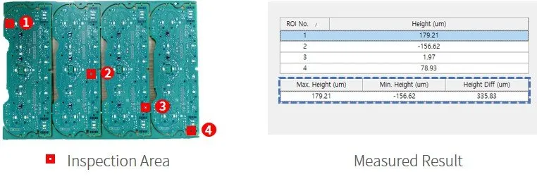
Warpage control is critical. Support large panels during reflow with carriers. Measure bow with a straightedge; exceed 1 mm signals redesign.
Troubleshooting Common Panelization Issues
Overly dense panels cause etchant starvation in centers. Solution: widen spacing or use spray etching. Warped panels from uneven cooling need annealing at 100 C for hours. Poor v-scores tear fibers; deepen to 1/3 board thickness.
Assembly shorts from tabs require insulated breaks. Fiducial misalignment shifts placement; recenter in layout. Scale panels gradually, starting small.
Conclusion
Mastering PCB panel size DIY unlocks efficient home etching panelization and small batch PCB assembly for hobbyists. From grasping factors like aspect ratio to applying simple PCB panel methods, thoughtful sizing yields reliable boards. Affordable panel size options abound for beginner PCB projects panel guidance, emphasizing balance over extremes. Adhere to standards for quality, test iteratively, and scale up confidently. Your next project will benefit from these insights, turning prototypes into polished builds.
FAQs
Q1: What is the ideal PCB panel size DIY for home etching?
A1: For home etching panelization, start with 6 by 8 inch panels to fit standard tanks and ensure even exposure. This size supports 8 to 12 small boards, minimizing warpage while maximizing yield. Add rails for handling. Adjust based on your bath agitation; larger risks uneven etch depths. Simple PCB panel methods like grid layouts work best here.
Q2: How do I choose affordable panel size options for small batch PCB assembly?
A2: Opt for 10 by 12 inch panels, common for fabricators handling small batches. They balance cost per board with shipping fees. Factor in v-scoring for easy depanelization. Check utilization over 80 percent for economy. Beginner PCB projects panel guidance recommends this for prototypes.
Q3: What are simple PCB panel methods for beginners?
A3: Use v-scoring or tab routing in your layout tool. Space boards 2 mm apart with edge rails. Export as one gerber set for etching or ordering. Depanel with shears post-process. This suits PCB panel size DIY without advanced tools.
Q4: Why does panel size affect beginner PCB projects panel guidance?
A4: Larger panels cut per-board costs but challenge home setups with warpage and handling. Smaller ones ease control for novices. Match to your tools for success in home etching panelization. Standards guide tolerances for reliability.





