 ALLPCB


Introduction
In PCB design, ensuring electrical safety requires careful attention to creepage distance, which defines the shortest path along the surface of an insulating material between two conductive parts. This parameter becomes critical in high-voltage applications where surface tracking can lead to failures. Material groups, determined by the comparative tracking index (CTI) of PCB substrates, directly influence the minimum required creepage distance. Engineers must select PCB materials with appropriate CTI values to comply with safety standards while optimizing board space. Understanding the interplay between creepage distance material groups and PCB material CTI helps prevent insulation breakdowns and enhances reliability. This article explores these concepts for electric engineers designing robust circuits.
Understanding Creepage Distance in PCB Design
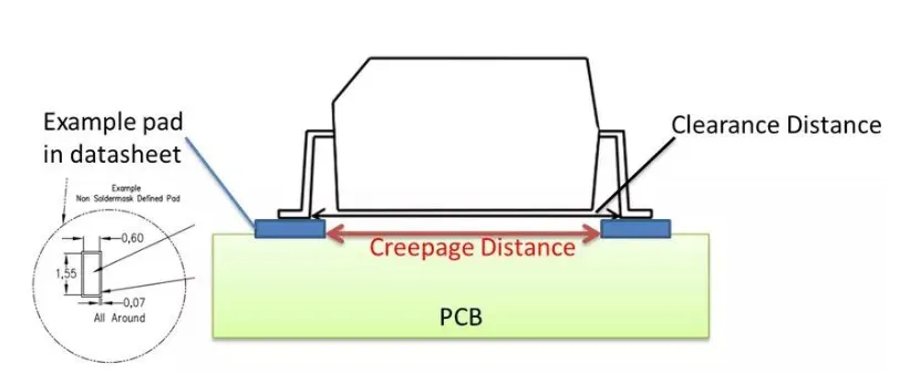
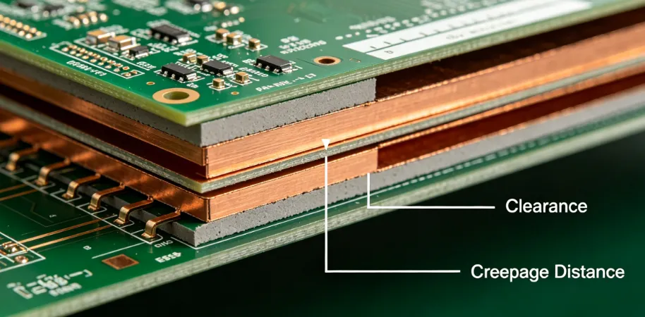
Creepage distance differs from clearance, which measures the straight-line air path between conductors; creepage follows the insulating surface, making it vulnerable to contamination and tracking. In polluted environments, moisture or dust can form conductive paths, reducing effective insulation. Standards like IEC 60664-1 provide guidelines for determining minimum creepage based on working voltage, pollution degree, and material properties. For PCBs, this ensures protection against overvoltages and maintains functional isolation. Electric engineers evaluate these distances early in layout to avoid redesigns. Proper creepage prevents arc flashovers and complies with safety certifications.
Pollution degree classifies environments from 1 (clean, no pollution) to 3 (industrial with conductive pollution). Higher degrees demand larger creepage distances to account for potential contaminants. Overvoltage categories further adjust requirements, with Category IV for fixed installations needing more spacing than Category I for electronics. Altitude affects air density, increasing distances above 2000 meters. These factors compound with material selection for comprehensive safety.
The Role of Comparative Tracking Index (CTI) in PCB Materials
PCB material CTI quantifies a substrate's resistance to electrical tracking, where carbonized paths form under voltage and contamination. Measured per industry methods, CTI indicates the voltage threshold before tracking occurs after repeated electrolyte drops. Higher CTI values mean better tracking resistance, allowing shorter creepage distances. This property is essential for creepage distance PCB material choices in dense layouts. Engineers specify CTI during material procurement to match application needs. Standard FR4 laminates vary in CTI, influencing overall board performance.
CTI testing simulates real-world surface degradation, applying voltage across electrodes on the material with a contaminating solution. The index reflects volts at which tracking fails after 100 drops. Materials with CTI above certain thresholds fall into defined groups, simplifying design calculations. This metric bridges material science and electrical safety in PCB engineering.
Material Groups and Their Impact on Creepage Distance
Creepage distance material groups categorize insulators by CTI ranges, standardizing minimum spacings across applications. Group I materials, with the highest CTI, permit the smallest creepage for a given voltage and pollution level. Group II offers moderate performance, while Groups IIIa and IIIb handle progressively harsher conditions but require larger distances. Selecting the right group optimizes space without compromising safety. In PCB design, datasheets list CTI to confirm group assignment.
IEC 60664-1 tables cross-reference voltage, pollution, and material group for precise creepage values. For example, higher groups demand up to double the spacing of Group I under identical conditions. This scaling accounts for tracking propensity. Engineers verify material group early to avoid qualification failures. Coated boards or conformal coatings can sometimes reduce effective requirements, but base material CTI remains foundational.
The relationship between CTI and creepage distance highlights trade-offs: premium high-CTI materials enable compact designs but cost more. Standard laminates often fall into Group IIIa or IIIb, suitable for most consumer electronics. Power supplies or medical devices may necessitate Group I for minimal spacing. Testing confirms group after processing, as lamination can alter properties.
Factors Influencing Creepage Distance Requirements
Beyond material groups, working voltage sets the baseline for creepage calculations. RMS or peak voltages determine insulation levels: basic, supplementary, or reinforced. Pollution degree adjusts for operational environments, with Degree 2 common for enclosed PCBs. Altitude correction factors increase distances proportionally above sea level. These variables ensure creepage distance PCB material selections align with real-world stresses.
Conformal coatings enhance effective CTI, potentially shifting material group equivalence. However, coatings add thickness and must be qualified separately. Solder masks provide partial protection but rely on base laminate CTI for primary safety. Engineers model these in simulation tools before fabrication. IPC-2221 offers PCB-specific spacing charts, complementing functional insulation standards.
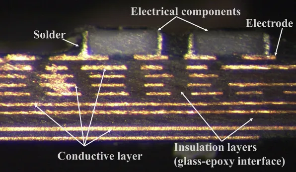
Environmental factors like humidity accelerate tracking, underscoring CTI importance. Vibration or thermal cycling can crack surfaces, exposing base material. Multi-layer boards require internal layer considerations, where clearance dominates over creepage. Holistic design integrates all parameters for certification success.
Related Read: Creepage Distance: Your Comprehensive Guide for PCB Design Safety
Best Practices for Selecting PCB Materials Based on CTI and Creepage
Start material selection by defining electrical requirements: voltage, insulation type, and environment. Consult supplier datasheets for verified CTI and group. Aim for the highest feasible CTI to minimize creepage distance material group penalties. Prototype testing validates performance under accelerated conditions. Document choices for compliance audits.
Layout strategies enhance safety: route high-voltage traces away from edges, use slots or grooves to extend creepage paths. Barriers like ribs increase effective distance without enlarging footprints. For high-density boards, high-CTI materials justify premium costs through space savings. Collaborate with fabricators on coating options to optimize.
Verification involves measurement post-fabrication, using calipers or optical tools for critical spacings. Hi-pot testing confirms isolation at overvoltages. Iterate if discrepancies arise from manufacturing tolerances. These practices ensure CTI and creepage distance integration yields safe, reliable PCBs.
Incorporate redundancy for critical applications, like double insulation. Monitor trends in material advancements for better CTI without Tg compromises. Balance cost, performance, and availability in procurement.
Related Reading: Beyond FR-4: Choosing High-Performance PCB Materials for Extended Lifespan
Troubleshooting Common Issues in Creepage and Material Selection
Engineers often overlook pollution degree mismatches, leading to undersized creepage. Review application notes against standards. Material CTI degradation from improper storage causes qualification fails; ensure dry conditions pre-lamination. High-frequency signals induce partial discharges, demanding conservative spacings.
Field failures from tracking trace to low-CTI choices in humid areas. Post-mortem analysis reveals carbon tracks. Solution: upgrade to Group I materials. Coating delamination exposes base laminate; select compatible processes. Systematic root-cause analysis refines future designs.
Simulation aids prediction: electromagnetic tools model field strengths along creepage paths. Correlate with CTI data for virtual qualification. These steps minimize iterations.
Conclusion
Creepage distance and material groups form the cornerstone of PCB safety, with CTI dictating feasible spacings. Selecting high-CTI materials reduces requirements, enabling compact, efficient designs. Adhering to standards like IEC 60664-1 ensures compliance and reliability. Electric engineers benefit from structured evaluation of voltage, pollution, and CTI interplay. Proactive choices prevent failures, optimize layouts, and meet certification. Prioritize these factors for superior performance.
FAQs
Q1: What is PCB material CTI and why does it matter for creepage distance?
A1: PCB material CTI, or comparative tracking index, measures an insulating substrate's resistance to surface tracking under voltage and contamination. Higher CTI values classify materials into better groups, allowing shorter creepage distances per standards. This directly impacts PCB material CTI selection for safety in high-voltage designs. Engineers use it to balance space and reliability, avoiding insulation breakdowns.
Q2: How does CTI and creepage distance relate in PCB design?
A2: CTI determines material groups that scale minimum creepage distance requirements based on working voltage and pollution degree. Per IEC guidelines, Group I (high CTI) permits smaller spacings than lower groups. CTI and creepage distance optimization enables denser layouts without safety risks. Verify via datasheets and testing for compliance.
Q3: What factors determine the creepage distance material group for a PCB?
A3: Creepage distance material group assignment relies on CTI testing results, categorizing from I (CTI ≥600) to IIIb (CTI 100-175). Voltage, pollution, and insulation level further influence required distances. Select groups matching application to minimize spacings logically. Standards provide tables for precise engineering decisions.
Q4: How to choose creepage distance PCB material for high-reliability applications?
A4: Prioritize materials with high CTI for creepage distance PCB material needs in harsh environments. Assess pollution degree, overvoltage category, and altitude. Use Group I or II for minimal spacings in power or medical PCBs. Validate with hi-pot tests and documentation for certification.
References
IEC 60664-1 - Insulation coordination for equipment within low-voltage systems. Part 1: Principles, requirements and tests. IEC.
IEC 60112 - Method for the determination of the comparative tracking index of solid insulating materials. IEC.
IPC-2221B - Generic Standard on Printed Board Design. IPC.


