 ALLPCB


Introduction
Polytetrafluoroethylene, or PTFE, serves as a premium substrate material in printed circuit boards designed for demanding applications. Engineers often face the challenge of balancing performance requirements with budget constraints when selecting PTFE PCBs over standard alternatives like FR4. These boards excel in high-frequency environments due to their low dielectric constant and minimal signal loss, making them essential for RF, microwave, and telecommunications systems. However, the elevated PTFE PCB price per square inch prompts scrutiny of whether the investment aligns with project goals. This article examines the primary PTFE PCB cost drivers, breaks down typical pricing, and evaluates PTFE PCB ROI through factory-driven perspectives. By understanding these elements, electrical engineers can make informed decisions that optimize both performance and economics.
What Are PTFE PCBs and Why Do They Matter?
PTFE PCBs utilize polytetrafluoroethylene as the core dielectric, offering a dielectric constant around 2.1 and dissipation factor below 0.0003 at microwave frequencies. This composition ensures stable electrical properties across wide temperature ranges and frequencies, unlike FR4 which exhibits higher losses above 1 GHz. In high-performance electronics, such as radar systems, 5G base stations, and satellite communications, signal integrity directly impacts system efficiency and reliability. Factory production of PTFE boards adheres to stringent standards like IPC-6012E to qualify rigid printed boards for these critical uses. Without PTFE, engineers risk signal attenuation, phase shifts, and crosstalk that degrade overall circuit performance. Thus, PTFE PCBs matter because they enable designs that meet exacting specifications in environments where standard materials fail.
The relevance extends to industries prioritizing low loss tangent for power efficiency and miniaturization. For instance, in automotive radar operating at 77 GHz, PTFE maintains impedance control better than alternatives, reducing redesign iterations. Procurement teams value this reliability, as it minimizes field failures and extends product lifecycles. From a manufacturing standpoint, PTFE demands specialized handling, yet delivers boards compliant with IPC-A-600K acceptability criteria. Engineers must weigh these benefits against costs to justify selection in prototypes or volume production.
Key PTFE PCB Cost Drivers
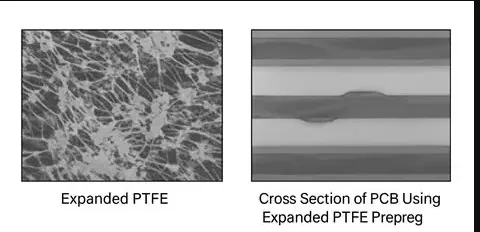
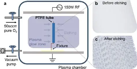
Material selection stands as the foremost PTFE PCB cost driver, with PTFE resin and reinforced laminates commanding premiums over FR4 fiberglass due to raw material scarcity and synthesis complexity.[1] Factories source pure PTFE or glass-filled variants, which inherently raise base costs by factors of 5 to 10 times compared to standard substrates. Processing challenges amplify this, as PTFE's non-stick surface resists copper adhesion, necessitating plasma etching or chemical treatments like sodium etch. Drilling precision suffers from material softness, leading to higher defect rates and scrap during via formation.
Layer count and board complexity further escalate expenses, with multilayer PTFE stacks requiring controlled lamination under vacuum to prevent voids. High-aspect-ratio vias demand specialized plating baths to ensure uniform copper deposition without delamination. Board size influences panel utilization efficiency; smaller panels yield less economically due to setup overheads. Volume orders mitigate per-unit costs through economies of scale, but low-volume prototypes incur high tooling and NRE charges. Tolerances for trace width, impedance, and thickness add to the tally, as metrology tools verify compliance with JEDEC standards for high-frequency qualification.
Additional factors include surface finishes suited for high-speed soldering and environmental testing for thermal cycling. Factories optimize yields by grouping similar designs, yet PTFE's sensitivity to contamination elevates cleanroom demands. Copper weight, typically 1 oz for RF traces, impacts etching precision and waste. Overall, these drivers create a multifaceted cost structure where upfront engineering controls long-term viability.
PTFE PCB Price per Square Inch: A Breakdown
Typical PTFE PCB price per square inch ranges from $2 to $10, starkly contrasting FR4's $0.10 to $0.50 span, depending on configuration and quantity.[2][3] For a standard 2-layer, 10x10 inch prototype panel, expect $200 to $500 total, scaling down with volume to $1.50 to $4 per square inch in thousands. Multilayer builds, common in RF modules, push prices toward the upper end due to sequential lamination cycles. High-frequency variants with filled PTFE for mechanical stability add 20-30% premiums.
Comparisons highlight disparities: a 4-layer FR4 board might cost $50 for the same area, while PTFE equivalents exceed $300 owing to material and process premiums.[2] Panelization efficiency matters; factories nest multiple boards to amortize setup, benefiting larger orders. Exotic finishes like ENIG for solderability incur extras, as do controlled impedance traces requiring TDR verification. Engineers quoting prototypes should specify stackup early to lock pricing.
- Material Type — Base $2-5; reinforced adds $1-3
- Layer Count — 2-layer: $2-4; 8+ layers: $6-10+
- Quantity — Prototype: $8-10; 1000+: $2-4
- Complexity (Vias, Traces) — Standard: baseline; HDI: +50%
Related Reading: A Practical Guide to Prototyping with PTFE PCBs: Tips and Best Practices
Justifying the Investment: PTFE PCB ROI Analysis
PTFE PCB ROI emerges from superior performance in high-frequency applications, where low insertion loss translates to reduced power draw and enhanced range. In a 5G antenna array, PTFE's dissipation factor under 0.001 minimizes heat, extending MTBF and slashing operational costs over FR4's higher losses. Factories observe fewer rework cycles post-assembly, as stable Dk prevents tuning adjustments. Lifecycle savings accrue from reliability; aerospace boards endure -55°C to 125°C without degradation, averting recalls.
Quantitative justification involves total cost of ownership: initial outlay recoups via 20-50% smaller footprints enabled by efficient signal propagation. Development time shortens, as simulations align closer to fabricated results. In volume telecom deployments, ROI materializes within 1-2 years through lower failure rates compliant with J-STD-020E moisture sensitivity. Engineers calculate break-even by modeling signal integrity metrics against alternatives.
Qualitative gains include faster time-to-market and competitive edges in specs-driven markets. While upfront PTFE PCB cost drivers dominate budgets, sustained benefits in efficiency and durability affirm the investment for qualifying designs.
Related Reading: PCB Cost Calculator: How to Estimate Your Project Budget
Best Practices for Managing PTFE PCB Costs
Optimize designs by minimizing layer count and via density while maintaining performance margins. Select glass-reinforced PTFE for cost-effective rigidity without pure resin premiums. Partner with factories experienced in PTFE to leverage yield data and avoid yield losses from improper handling. Standardize stackups across projects to reduce engineering NRE.
Volume planning secures discounts; commit to panels over singles for 30-50% savings. Simulate impedance early to eliminate iterations. Adhere to IPC guidelines during layout to prevent tolerance-driven upcharges. Test prototypes rigorously to validate ROI before scaling.
Incorporate hybrid stacks with FR4 cores where feasible, reserving PTFE for critical signal layers. These practices align factory capabilities with engineering needs, maximizing value.
Conclusion
PTFE PCBs command higher prices due to premium materials and fabrication intricacies, yet deliver indispensable value in high-performance electronics. Key PTFE PCB cost drivers like processing and complexity underscore the need for strategic design. Typical PTFE PCB price per square inch reflects this, but ROI calculations reveal long-term savings in reliability and efficiency. Electrical engineers benefit from factory insights emphasizing standards compliance and optimization tactics. Ultimately, investing in PTFE justifies itself where signal integrity defines success, ensuring robust systems in RF and beyond.
FAQs
Q1: What factors primarily influence PTFE PCB price per square inch?
A1: PTFE PCB price per square inch hinges on material purity, layer count, and processing needs like plasma etching for adhesion. Reinforced variants cost less than pure PTFE, while prototypes exceed $5 due to low volumes. Factories factor board size and tolerances, with economies kicking in above 100 units. Comparing to FR4 highlights 5-10x premiums driven by low-loss properties.
Q2: How do PTFE PCB cost drivers compare to standard materials?
A2: PTFE PCB cost drivers include expensive laminates and specialized drilling, unlike FR4's straightforward processes. Adhesion treatments and cleanroom handling elevate expenses by 300-500%. Multilayers amplify this due to lamination challenges. Volume mitigates impacts, but high-frequency tolerances add consistently. Engineers prioritize these for performance trade-offs.
Q3: What is the typical PTFE PCB ROI in high-frequency applications?
A3: PTFE PCB ROI stems from minimal signal loss, enabling compact designs and lower power use in RF systems. Lifecycle gains from thermal stability offset initial costs within 1-2 years via reduced failures. Compliance with standards like IPC-6012E ensures reliability. High-volume telecom sees fastest returns through efficiency.
Q4: How can engineers reduce PTFE PCB costs without sacrificing performance?
A4: Panelize designs for efficient utilization and standardize stackups to cut NRE. Use hybrids with FR4 where signals permit, reserving PTFE for critical paths. Select factories with PTFE expertise for higher yields. Early impedance simulation avoids redesigns. Volume commitments yield 40% savings.
References
[1] https://blog.epectec.com/ptfe-vs-fr4-pcb-laminate-materials-cost-and-performance-options
[2] https://resources.pcb.cadence.com/blog/er-part-1-pcb-substrates-the-truth-about-cost-vs-performance-in-2025
[3] https://www.kingsunpcb.com/average-pcb-manufacturing-cost-2020-2025


