 ALLPCB


Introduction
Rigid-flex PCB stackup design combines rigid and flexible substrates to enable compact, reliable electronics in applications like wearables, medical devices, and aerospace systems. Engineers must balance mechanical flexibility with electrical performance to prevent failures such as delamination or signal distortion. Proper stackup configuration ensures the board withstands repeated bending while maintaining signal integrity and manufacturability. This article explores rigid-flex PCB stackup rules, examples, and optimization strategies for impedance control, signal integrity, and design for manufacturability (DFM). By following structured principles, designers can achieve high reliability without compromising functionality. Understanding these elements is crucial for electric engineers tackling complex, space-constrained designs.
What Is Rigid-Flex PCB Stackup and Why It Matters
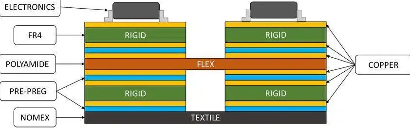
A rigid-flex PCB stackup defines the layered arrangement of materials, copper foils, and dielectrics that form both rigid and flexible sections of the board. Flex areas use polyimide substrates with coverlay protection, while rigid sections employ standard laminates like FR-4. The stackup specifies thicknesses, copper types, and bonding methods to integrate these regions seamlessly. This hybrid construction matters because it allows three-dimensional packaging, reducing connectors and improving reliability in dynamic environments.
In high-performance applications, poor stackup design leads to warpage, cracking during bends, or impedance mismatches that degrade signals. For electric engineers, optimizing the stackup directly impacts overall system performance, especially in high-speed interfaces. Industry standards like IPC-2223C guide these designs to ensure mechanical durability and electrical consistency. Effective stackups minimize stress concentrations at transitions and support controlled impedance across the entire board.
Key Technical Principles of Rigid-Flex PCB Stackup Design
Symmetry forms the foundation of rigid-flex PCB stackup design, with flex layers positioned centrally to balance bending moments and prevent curl or warpage. Engineers achieve this by mirroring dielectric thicknesses and copper weights around the neutral axis. Adhesiveless flex cores are preferred for dynamic applications to avoid adhesive flow issues that stiffen the flex region. No-flow prepregs at rigid-flex interfaces prevent resin invasion, maintaining flexibility.
Layer configuration limits flex sections to even numbers, typically one or two layers for optimal bend performance. Rolled annealed copper suits flex areas due to its ductility, while electrodeposited copper works for rigid zones. Ground planes in flex regions use hatched patterns rather than solid fills to reduce stiffness. Transition zones require careful planning, with traces fanned out into teardrops to distribute mechanical stress.
Bend mechanics dictate stackup choices, as repeated flexing induces copper fatigue if layers exceed recommended counts. Bookbinding constructions, where flex layers slide independently in bend areas, enable tighter radii without bonding. These principles ensure the stackup supports both static and dynamic use cases reliably.
Rigid-Flex PCB Stackup Rules and Best Practices
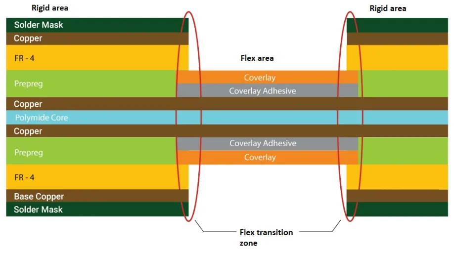
Rigid-flex PCB stackup rules emphasize even layer counts with flex cores in the stack center to minimize deformation. Traces must run perpendicular to bend lines, staggered between layers to avoid alignment stress. Vias and pads stay clear of bend and transition zones by defined keepouts, preventing barrel cracking from CTE mismatches. Coverlay protects exposed flex conductors, with selective application to avoid rigid areas.
Best practices include specifying copper types explicitly: rolled annealed for flex ductility and electrodeposited for rigid efficiency. Hatched ground planes in flex sections enhance flexibility without sacrificing shielding. Engineers document stackups graphically, noting material specs per IPC standards for equivalents. These rules reduce common violations like sharp trace angles or insufficient annular rings that lead to peeling.
For multilayer flex, bookbinding techniques unbond layers in bend zones, allowing independent movement. Stiffeners reinforce component areas near flex, distributing solder joint loads. Adhesive thicknesses in rigid bonds stay below 10% of total construction to control roughness and ensure lamination integrity.
Optimizing Rigid-Flex PCB Stackup Impedance Control
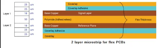
Rigid-flex PCB stackup impedance control requires precise dielectric spacing and symmetric layering to maintain consistent characteristic impedance across rigid and flex transitions. Thicker flex cores support target values like 50-ohm single-ended or 100-ohm differential pairs, but increase overall board thickness. Reference planes must continue through flex areas as hatched planes to minimize discontinuities. Trace widths and spacings adjust based on material dielectric constants, with polyimide offering suitable performance below 10 GHz.
Challenges arise from varying material properties, so stackups use low-flow prepregs to preserve spacings during lamination. Simulation verifies impedance profiles, accounting for flex bending effects on dielectric air gaps. Ground plane integrity prevents crosstalk, with via stitching securing returns. These strategies ensure impedance tolerances hold post-fabrication.
DFM integrates impedance coupons in stackup drawings, specifying widths, heights, and tolerances. Symmetric builds around signal layers reduce variations from warpage. Electric engineers prioritize continuous reference planes for high-speed signals transitioning through flex.
Ensuring Signal Integrity in Rigid-Flex PCB Stackup
Rigid-flex PCB stackup signal integrity hinges on uniform impedance and minimal discontinuities at material interfaces. Flex sections introduce challenges like thinner dielectrics and bend-induced variations, so centered flex layers maintain plane proximity. Routing avoids 90-degree bends in high-speed nets, using curved transitions at least three times trace width. Differential pairs stay paired through transitions, with length matching to control skew.
Shielding employs ground pours or planes adjacent to signals, hatched in flex for compliance. Via transitions use back-drilling or blind vias to shorten stubs, preserving return paths. Stackup symmetry curbs crosstalk by balancing coupling. Testing validates eye diagrams across operating bends.
Transition zones demand fanouts and anchors to secure traces against peel. These practices sustain signal quality in compact, folded assemblies.
DFM Considerations for Rigid-Flex PCB Stackup
Rigid-flex PCB stackup DFM focuses on manufacturability by enforcing via exclusions in bend radii and transitions per IPC-2223C guidelines. Minimum clearances, like drill-to-copper at least 8 mils, prevent plating shorts in flex. No-flow prepregs and adhesiveless cores simplify lamination, avoiding flex stiffening. Stackup notes specify RA copper for dynamic flex and tolerances like ±30-50 μm finished thickness.
Symmetry prevents warpage during reflow, critical for assembly yields. Prototype bend testing qualifies dynamic designs before production. Fabricator reviews confirm material compatibility and process margins. These steps optimize yield and reliability.
Rigid-Flex PCB Stackup Examples
Common rigid-flex PCB stackup examples include a 4-layer build with two central flex layers bonded between rigid FR-4 sections. The flex core uses polyimide with RA copper, coverlay on outer surfaces, and no-flow prepreg at interfaces. This suits static bend-to-install applications, centering signals for impedance control.
An 8-layer example adds rigid multilayers outer, with bookbinding in flex tails for repeated flexing. Hatched grounds flank signals, staggered traces enhance durability. Transition keepouts fan traces into pads.
A high-speed 6-layer stackup embeds stripline signals between planes, using low-Dk polyimide in flex for 100-ohm pairs. These examples illustrate rules scaling with complexity.
Conclusion
Rigid-flex PCB stackup design optimizes performance by prioritizing symmetry, material selection, and transition integrity. Adhering to rules for bends, vias, and impedance ensures signal integrity and DFM success. Electric engineers benefit from IPC-6013D qualification paths for proven reliability. Implementing these principles yields robust boards for demanding applications. Future designs will leverage advanced simulations for even tighter integrations.
FAQs
Q1: What are essential rigid-flex PCB stackup rules for beginners?
A1: Rigid-flex PCB stackup rules require centering flex layers symmetrically, using even layer counts, and placing traces perpendicular to bends. Vias avoid bend zones, with hatched grounds in flex for flexibility. RA copper suits dynamic flex, per IPC-2223C. These prevent cracking and warpage, easing DFM.
Q2: How does rigid-flex PCB stackup impedance control affect high-speed designs?
A2: Rigid-flex PCB stackup impedance control uses symmetric dielectrics and continuous reference planes to hold 50/100-ohm targets. Thicker cores and trace adjustments compensate flex variations. Simulations verify post-bend integrity, minimizing crosstalk for signals over 10 Gbps.
Q3: Why is signal integrity critical in rigid-flex PCB stackup?
A3: Rigid-flex PCB stackup signal integrity prevents discontinuities at transitions via fanouts and blind vias. Staggered traces and shielding reduce EMI. Symmetric builds maintain impedance, ensuring clean eye patterns in folded assemblies.
Q4: What DFM tips improve rigid-flex PCB stackup manufacturability?
A4: Rigid-flex PCB stackup DFM tips include no-flow prepregs, via keepouts, and thickness tolerances of ±30-50 μm. Specify materials per IPC standards and review with fabricators. Symmetry curbs warpage, boosting yields.
References
IPC-2223C — Sectional Design Standard for Flexible Printed Boards. IPC, 2011
IPC-6013D — Qualification and Performance Specification for Flexible/Rigid-Flexible Printed Boards. IPC, 2017


