ALLPCB


Introduction
Polytetrafluoroethylene, or PTFE, serves as a preferred substrate material for high-frequency printed circuit boards due to its exceptionally low dielectric constant and dissipation factor. These properties enable superior signal integrity in applications such as radar systems, telecommunications, and satellite communications. However, the PTFE PCB manufacturing process introduces unique hurdles that demand specialized techniques and precise control. Among the most critical challenges are dimensional instability, which can lead to misalignment during assembly, and poor solder mask adhesion, which compromises board protection and reliability. PTFE PCB drilling issues further complicate production by generating material smear and rough hole walls. Engineers must address these obstacles to achieve consistent performance in demanding environments, aligning with rigorous industry standards for quality and functionality.
The push for higher operating frequencies in modern electronics amplifies the need for reliable PTFE-based boards. While standard FR-4 materials suffice for lower speeds, PTFE excels where minimal signal loss is paramount. Yet, its inherent material characteristics, including softness and chemical inertness, create friction in fabrication workflows. This article explores the root causes of these challenges and outlines proven strategies to mitigate them. By understanding the PTFE PCB manufacturing process intricacies, electrical engineers can optimize designs for manufacturability and enhance yield rates. Factory-driven insights reveal that proactive process controls make all the difference in overcoming these persistent issues.
Why PTFE PCBs Matter and Their Unique Challenges
PTFE PCBs stand out in high-frequency applications because of their stable electrical properties across wide frequency ranges, typically up to millimeter waves. The material's low loss tangent ensures signals propagate with minimal attenuation, critical for phased array antennas and 5G infrastructure. Industry relevance stems from growing demands in aerospace, defense, and wireless systems, where even minor performance degradation can cascade into system failures. However, transitioning from design to production reveals PTFE's mechanical drawbacks compared to rigid epoxies. Dimensional instability arises from the polymer's viscoelastic behavior, leading to creep under thermal stress and handling.
Solder mask adhesion problems trace back to PTFE's non-polar surface, which repels liquid photoimageable masks commonly used in PCB fabrication. Drilling exacerbates these issues, as the soft matrix generates heat and debris that smear into vias, obstructing plating. These factors elevate scrap rates and extend lead times in the PTFE PCB manufacturing process. Electrical engineers benefit from recognizing these pain points early, allowing for design adjustments that accommodate material limitations. Standards like IPC-6018 provide qualification criteria tailored to high-frequency boards, emphasizing dimensional control and surface integrity. Ultimately, mastering these challenges unlocks PTFE's full potential for next-generation electronics.
Related Reading: PTFE PCB Materials: Understanding Dielectric Constant and Loss Tangent
Technical Principles Behind Dimensional Instability in PTFE PCBs
Dimensional instability in PTFE PCBs primarily stems from the material's high coefficient of thermal expansion, particularly in the Z-axis, which mismatches copper foil properties. During lamination and subsequent thermal cycling, this differential expansion induces stresses that cause warpage or bowing. Pure PTFE's low modulus of elasticity, around 0.5 GPa, allows it to deform easily under compressive forces, unlike reinforced epoxies. Fillers such as glass fibers or ceramics mitigate this by increasing rigidity, but even filled variants require controlled cooling rates to prevent microcracks. Moisture absorption plays a minimal role due to PTFE's hydrophobic nature, yet process-induced voids can amplify instability.
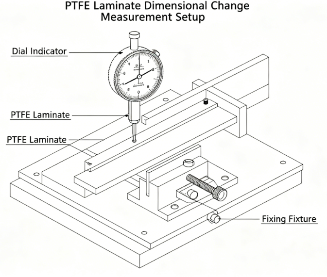
The mechanism involves polymer chain relaxation over time, known as creep, which alters feature spacing and impacts impedance consistency. In multilayer stacks, core shifts occur if lamination pressures exceed optimal ranges, leading to registration errors beyond 0.1 mm. Electrical engineers observe this during assembly when components misalign with pads. Testing per IPC-TM-650 methods quantifies bow and twist, setting thresholds for acceptability. Understanding these principles guides the selection of preconditioning steps, such as baking panels before drilling. Factory experience shows that symmetric stackups and edge clamping during pressing minimize these effects, preserving signal paths.
Related Reading: A Practical Guide to Prototyping with PTFE PCBs: Tips and Best Practices
PTFE PCB Drilling Issues: Causes and Mechanisms
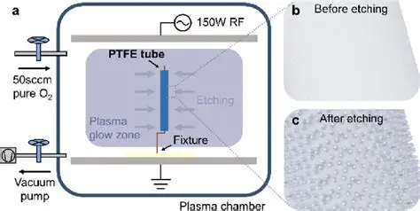
The PTFE PCB drilling issues originate from the material's low hardness and high ductility, which cause drill bits to wander and generate excessive smear. Conventional high-speed steel drills overheat the soft resin, melting it and depositing it on hole walls, which impedes electroless copper plating. Burrs form at entry and exit points due to insufficient chip evacuation, especially in aspect ratios above 6:1. Laser drilling faces incomplete ablation, leaving carbon residue that requires aggressive desmear. These problems degrade via reliability, increasing open circuits or barrel cracks under thermal shock.
Heat buildup during mechanical drilling exacerbates smear because PTFE's melting point nears 327 degrees Celsius, yet friction generates localized temperatures close to that threshold. Engineers note that spindle speeds above 100,000 RPM without peck cycles worsen deflection in thin webs. Plasma desmear etches away debris using oxygen radicals, but over-etching roughens surfaces, affecting plating adhesion. Standards like IPC-6012 specify hole wall quality criteria, including maximum roughness and no smear. Process parameters, such as chipload under 0.001 mm/rev, prove essential for clean holes. Addressing these PTFE PCB drilling issues early prevents downstream failures in high-frequency performance.
Solder Mask Adhesion Challenges in PTFE PCB Manufacturing
PTFE PCB solder mask adhesion falters due to the substrate's low surface energy, typically below 20 mN/m, which prevents wetting by standard liquid photoimageable soldermasks. The inert fluoropolymer surface resists chemical bonding, leading to delamination during reflow or humidity exposure. Post-etch residues further contaminate traces, compounding peel-off risks. Manufacturers observe bubbles or lifting after UV curing if application delays exceed tight windows. This challenge impacts conformal coating compatibility and overall board protection against ionic contamination.
Surface activation via plasma treatment introduces reactive groups like peroxides, boosting adhesion energy without altering bulk properties. Chemical etching with sodium naphthalenide solutions roughens the surface selectively, creating mechanical interlocks. Timing proves critical: masks must apply within hours of etching to exploit fresh oxide layers on copper. Curing profiles demand low ramp rates to avoid thermal expansion mismatches. IPC-A-600 acceptability criteria guide visual inspections for adhesion integrity. Electrical engineers specify these steps in fabrication notes to ensure robust environmental resistance.
Best Practices for Overcoming PTFE PCB Manufacturing Challenges
Integrating best practices into the PTFE PCB manufacturing process starts with material selection, favoring filled composites for balanced stability. Lamination employs vacuum-assisted pressing at 350-380 degrees Celsius with dwell times exceeding 2 hours to expel volatiles and ensure uniform flow. Pre-baking panels at 120 degrees Celsius for 4 hours preconditions the stack, reducing outgassing. For drilling, carbide or diamond-coated tools with entry materials prevent burrs, combined with multiple peck depths for debris clearance. Post-drill plasma cycles at 200-500 W for 10-20 minutes optimize hole quality.
Solder mask adhesion improves through sequential plasma cleaning followed by immediate mask application, using formulations with adhesion promoters. Multilayer alignment relies on fiducials and optical registration systems tolerant of 50-micron shifts. Quality checks include thermal cycle testing per J-STD-020 to verify stability. Factory protocols emphasize cleanroom handling to avoid particulate-induced defects. Electrical engineers collaborate on design rules like wider annular rings to buffer tolerances. These measures align with IPC-6018 performance specs, yielding boards with under 0.75% bow and twist.
Troubleshooting Insights for Electrical Engineers
Common troubleshooting begins with warpage exceeding limits: inspect lamination logs for asymmetric builds and re-laminate with cauls. If PTFE PCB drilling issues persist, audit chipload and vacuum hold-down; switch to CO2 lasers for microvias. Solder mask delamination signals inadequate activation, remedied by etch verification via contact angle tests under 30 degrees. Via opens trace to smear residue, confirmed by cross-section microscopy, necessitating desmear validation. Layer misalignment calls for X-ray inspection and adjusted drill offsets.
Process data logging reveals patterns, such as seasonal humidity spikes affecting stability. Engineers adjust bake times accordingly. Yield analytics highlight drill wear after 500 hits, prompting frequent changes. Collaboration with fabricators ensures DFM reviews catch issues pre-production. These factory-driven tactics restore reliability without redesigns.
Conclusion
Overcoming dimensional instability and solder mask adhesion in PTFE PCB manufacturing demands a holistic approach rooted in material science and process precision. By tackling drilling issues through optimized parameters and surface treatments, engineers achieve high yields and performance. Standards like IPC-6018 and IPC-6012 frame these efforts, ensuring compliance and repeatability. Electrical professionals gain from proactive design-for-manufacturability, balancing PTFE's electrical advantages with mechanical realities. As high-frequency demands escalate, refined PTFE PCB manufacturing processes will drive innovation in critical applications. Investing in these solutions positions teams for success in complex projects.
FAQs
Q1: What are the main PTFE PCB drilling issues encountered in manufacturing?
A1: PTFE PCB drilling issues include excessive smear from material softness, burr formation, and drill wander due to low rigidity. These arise during mechanical or laser processes, obstructing plating and raising impedance errors. Mitigation involves peck drilling, specialized tools, and plasma desmear to clean hole walls effectively. Standards guide acceptable roughness levels for reliable vias.
Q2: How can engineers improve PTFE PCB solder mask adhesion?
A2: PTFE PCB solder mask adhesion improves via plasma or chemical surface activation to increase wettability. Apply masks promptly after etching, within process windows, using promoter-enhanced formulations. Verify adhesion through tape tests and thermal cycling. This prevents delamination, enhancing protection in humid environments.
Q3: Why does dimensional instability occur in the PTFE PCB manufacturing process?
A3: Dimensional instability in the PTFE PCB manufacturing process results from high CTE mismatch, creep, and low modulus. Thermal lamination induces warpage if cooling is uncontrolled. Filled materials and symmetric stacks counteract this, meeting IPC specs for bow and twist. Design symmetry aids stability.
Q4: What role do standards play in addressing PTFE manufacturing challenges?
A4: Standards like IPC-6018 and IPC-6012 define qualification for high-frequency PTFE boards, specifying dimensional tolerances and surface quality. They guide testing for warpage, hole integrity, and adhesion. Compliance ensures manufacturability and performance in demanding applications.
References
IPC-6018 — Qualification and Performance Specification for High Frequency (Microwave) Printed Boards. IPC.
IPC-6012E — Qualification and Performance Specification for Rigid Printed Boards. IPC, 2017.
IPC-A-600K — Acceptability of Printed Boards. IPC, 2020.
J-STD-020E — Moisture/Reflow Sensitivity Classification. JEDEC, 2014