ALLPCB


Introduction
The PCB industry faces increasing pressure from environmental regulations and sustainability demands, prompting engineers to evaluate alternative materials. Halogen-free PCBs emerge as a key option, offering reduced toxicity during manufacturing and end-of-life processing. However, the halogen-free PCB cost often exceeds that of conventional boards, raising questions about viability. This PCB cost analysis explores upfront expenses alongside long-term factors like compliance and reliability. Factory-driven insights highlight how PCB manufacturing cost evolves with material choices. Ultimately, assessing total cost of ownership reveals whether halogen-free options align with project goals.
What Is a Halogen-Free PCB and Why Does It Matter?
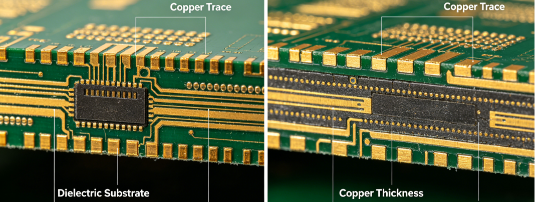
Halogen-free PCBs use base materials, such as laminates and prepregs, with minimal chlorine and bromine content. Industry definitions typically limit chlorine and bromine to less than 900 parts per million each, with total halogens under 1500 parts per million. These thresholds ensure low environmental persistence and safer combustion byproducts. Flame retardancy shifts from brominated or chlorinated compounds to phosphorus or nitrogen-based alternatives. Electrical engineers prioritize these boards for applications in consumer electronics, automotive, and telecommunications where regulatory compliance is critical.
Environmental regulations drive adoption, as frameworks like RoHS and REACH restrict certain halogenated substances to curb hazardous waste. While not all regulations mandate full halogen elimination, market trends and customer specifications increasingly favor these materials. Factory production benefits from cleaner processing, reducing corrosion risks on equipment. Reliability improves in humid environments due to lower hygroscopicity in some formulations. For procurement teams, specifying halogen-free aligns with corporate sustainability goals without compromising performance.
Technical Principles Behind Halogen-Free PCBs
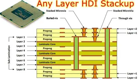
Halogen-free laminates maintain FR-4 like properties but substitute traditional flame retardants. Phosphorus-based systems provide char formation during combustion, suppressing flame spread effectively. Nitrogen compounds enhance thermal stability, aiding multilayer stackups. These changes influence dielectric constants and loss tangents minimally, preserving signal integrity for high-speed designs. Manufacturers qualify materials through standardized thermal stress tests to verify delamination resistance.
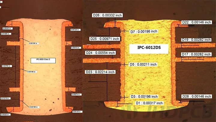
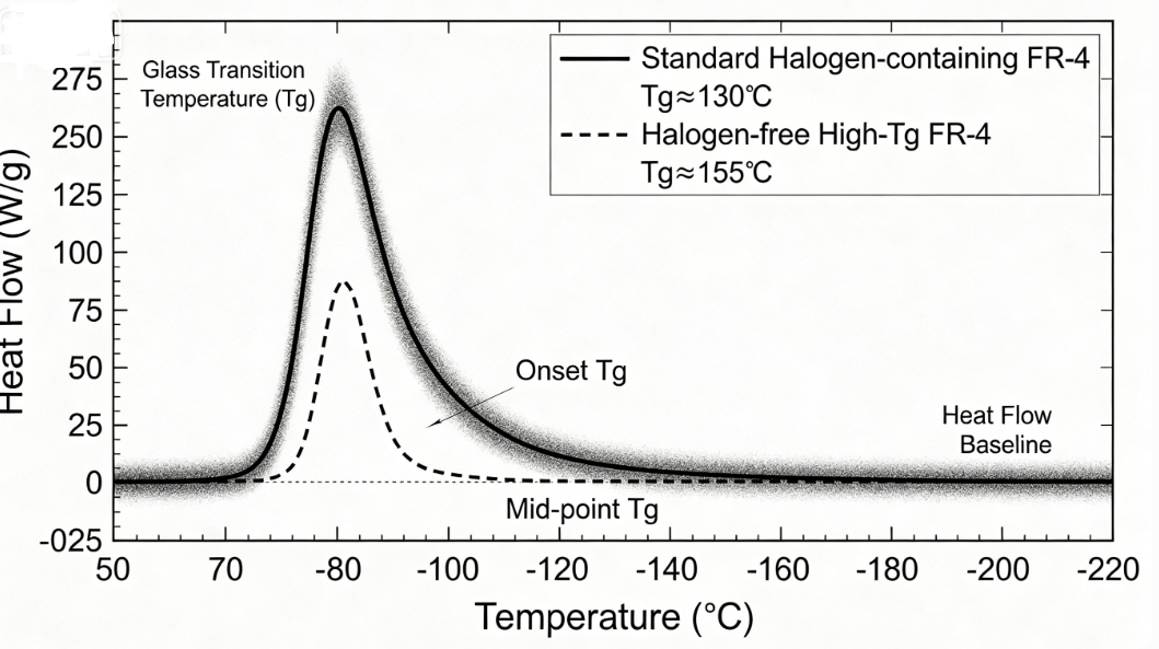
Processing differences arise during lamination and drilling, where alternative resins may require adjusted pressure and temperature profiles. Solder mask and silkscreen formulations also adopt halogen-free inks to meet overall board specifications. As per IPC/JEDEC J-STD-609A, boards meeting criteria receive "HF" labeling for traceability. Electrical performance remains comparable, with glass transition temperatures often matching or exceeding standard FR-4. Factory experience shows consistent yields when suppliers validate materials upfront.
Moisture sensitivity demands attention, as some halogen-free prepregs absorb slightly more during storage. Proper baking per JEDEC J-STD-020E prevents reflow defects like popcorn cracking. Corrosion resistance improves, minimizing ionic residues that plague halogenated boards in assembly. These principles underscore why halogen-free options suit lead-free soldering processes prevalent today.
Related Reading: Top 5 Misconceptions About Halogen Free PCB Manufacturing
Breaking Down PCB Manufacturing Cost for Halogen-Free Boards
Material selection dominates halogen-free PCB cost, as specialized laminates command premiums over standard FR-4. Resin formulations and additives elevate raw input prices, passed to customers in quotes. However, volume production amortizes this differential, narrowing gaps for high-mix runs. Tooling and setup remain unchanged, focusing expenses on procurement. Factories optimize by stocking qualified halogen-free cores for rapid turnaround.
Fabrication steps like etching and plating proceed similarly, with no major yield penalties once processes stabilize. Multilayer builds may incur minor adjustments for inner layer registration due to CTE variations. Surface finishes, such as ENIG or OSP, apply universally without cost hikes. Testing verifies compliance through halogen content analysis, adding nominal lab fees. Overall, PCB manufacturing cost rises 10 to 20 percent upfront, but economies scale with demand.
Assembly considerations factor into total evaluation. Halogen-free boards exhibit lower smoke density in rework scenarios, easing operator safety. Compatibility with no-clean fluxes reduces cleaning steps. Long-term field reliability cuts warranty claims from corrosion failures.
Related Reading: Decoding PCB Manufacturing Costs: A Comprehensive Guide for 2025
PCB Cost Analysis: Upfront vs. Total Cost of Ownership
Short-term PCB cost analysis reveals higher quotes for halogen-free prototypes, deterring low-volume projects. Engineers must project volumes to justify premiums. Material volatility affects pricing, though stable supply chains mitigate swings. Compliance documentation adds administrative overhead initially.
Total cost of ownership shifts the equation favorably. Environmental regulations impose penalties or redesigns for non-compliant boards, inflating future expenses. Recycling streams prefer halogen-free waste, lowering disposal fees under waste directives. Enhanced durability extends product lifecycles, deferring replacements.
Factory data indicates fewer rejects from humidity-induced defects, boosting throughput. Qualification per IPC-TM-650 methods confirms performance parity, avoiding costly requalifications. Supply chain resilience grows as halogen-free availability expands globally. Procurement teams calculate TCO by summing acquisition, operation, and end-of-life costs.
- Material Acquisition — Halogenated PCB: Lower baseline; Halogen-Free PCB: Higher premium.
- Manufacturing Yield — Halogenated PCB: Standard; Halogen-Free PCB: Comparable post-optimization.
- Compliance Certification — Halogenated PCB: Basic RoHS; Halogen-Free PCB: Full env alignment.
- Lifecycle Maintenance — Halogenated PCB: Higher corrosion risk; Halogen-Free PCB: Reduced failures.
- Disposal/Recycling — Halogenated PCB: Restricted streams; Halogen-Free PCB: Preferred processing.
Best Practices for Implementing Halogen-Free PCBs
Select suppliers with proven halogen-free portfolios and material data sheets. Specify limits explicitly in purchase orders, referencing IEC 61249-2-21 for resin specs. Conduct design reviews for CTE matching in stackups to prevent warpage. Prototype early to baseline process windows.
Storage protocols mirror standard boards: dry cabinets below 5 percent RH. Assembly lines calibrate reflow profiles for peak temperatures up to 260 degrees Celsius. Post-process inspections check for white spots or brittleness, common myths debunked by proper handling. Factories recommend phosphorus-based over nitrogen for high-Tg needs.
Volume forecasting secures better pricing tiers. Hybrid panels blend halogen-free and standard for cost testing. Sustainability audits quantify TCO savings annually.
Factory Insights: Real-World Cost Trade-Offs
From a manufacturing standpoint, transitioning to halogen-free requires resin qualification runs, amortizing over production. Yields stabilize after 10 to 20 panels, matching FR-4 benchmarks. Automotive and medical sectors mandate these for toxicity profiles, driving internal adoption. Engineers report neutral performance in signal loss tests.
Regulatory foresight prevents last-minute changes, as seen in REACH updates. Collaborative supplier audits ensure traceability. Long-term, halogen-free reduces CAPEX on ventilation for less corrosive fumes.
Conclusion
Halogen-free PCB cost presents an initial hurdle, but PCB cost analysis underscores value in regulated markets. Environmental regulations and reliability gains tip total cost of ownership toward investment worthiness. Factory practices confirm manufacturability parity with proactive design. Electrical engineers benefit from balancing upfront premiums against lifecycle economies. Adopting these materials positions projects for future compliance seamlessly.
FAQs
Q1: What drives the higher halogen-free PCB cost compared to standard boards?
A1: Halogen-free PCB cost stems primarily from specialized laminates using phosphorus or nitrogen flame retardants instead of cheaper brominated compounds. PCB manufacturing cost includes qualification testing and limited supplier scales. However, as demand grows, premiums narrow for mid-to-high volumes. Total cost of ownership often offsets this through compliance savings and recycling ease. Factories advise volume commitments for optimal pricing.
Q2: How do environmental regulations impact PCB cost analysis?
A2: Environmental regulations like RoHS and REACH restrict halogenated substances, pushing halogen-free adoption to avoid fines or redesigns. PCB cost analysis must factor certification and documentation expenses. Non-compliance risks supply chain disruptions, elevating indirect costs. Halogen-free options streamline global market access. Engineers gain by integrating regs early in design.
Q3: Is the total cost of ownership lower for halogen-free PCBs?
A3: Total cost of ownership for halogen-free PCBs decreases via reduced corrosion, simpler recycling, and regulatory avoidance. Initial PCB manufacturing cost rises modestly, but field reliability cuts maintenance. Factory insights show fewer defects in humid applications. Long-term projections favor halogen-free for high-volume, regulated products. Procurement evaluates TCO holistically.
Q4: When should electrical engineers choose halogen-free PCBs?
A4: Opt for halogen-free PCBs in automotive, consumer, or medical apps under environmental regulations. PCB cost analysis justifies for volumes over prototypes where TCO shines. Standard boards suffice for internal tools without compliance needs. Factory alignment ensures performance matches specs.
References
IEC 61249-2-21 — Requirements for halogen-free epoxy resin based laminates. IEC.
IPC/JEDEC J-STD-609A — Marking and Labeling of Components, PCBs and Subassemblies. IPC/JEDEC.