ALLPCB


If you're new to PCB design, you might be wondering how to ensure your board works correctly and can be manufactured without issues. The answer lies in constraint management—a key part of the design process that sets rules and limits to guide your layout and routing. In this guide, we'll introduce PCB design constraints for beginners, explain basic PCB design rules, and provide simple PCB design guidelines to help you get started. Whether you're learning about introduction to constraint management or exploring PCB design software constraints, this post will break it all down in an easy-to-understand way.
Designing a printed circuit board (PCB) is like solving a complex puzzle. Every component, trace, and connection must fit together perfectly while meeting electrical, physical, and manufacturing requirements. Without proper constraints, your design could face issues like signal interference, overheating, or even failure during production. Let’s dive into the world of constraint management and learn how to create better PCB designs from the ground up.
What Is Constraint Management in PCB Design?
Constraint management in PCB design is the process of defining and applying rules or limits that control how your board is laid out and how signals behave. These rules ensure that your design meets performance goals, fits within physical boundaries, and can be manufactured without errors. For beginners, think of constraints as a set of guidelines that prevent mistakes and keep your design on track.
Constraints cover a wide range of factors, such as the spacing between traces, the width of traces for specific currents, and the placement of components to avoid interference. By setting these rules early in the design process, you can avoid costly redesigns and ensure your PCB works as intended. Constraint management is often handled within design software, where you can input specific values and let the tool check for violations as you work.
Why Are Constraints Important for Beginners?
As a beginner, you might be tempted to skip constraints and just start placing components and routing traces. However, this can lead to problems like electrical noise, overheating, or boards that can't be manufactured. Constraints act as a safety net, helping you avoid common pitfalls. They also save time by catching errors early, before you send your design for production.
For example, if you're designing a board with high-speed signals, a constraint might require a trace length of no more than 50 mm to prevent signal delay issues. Without this rule, you might create a trace that's too long, causing your circuit to fail. Constraints ensure your design is reliable and manufacturable from the start.
Understanding Basic PCB Design Rules
Before diving deeper into constraint management, let’s cover some basic PCB design rules that form the foundation of a good design. These rules are often the starting point for setting constraints in your software.
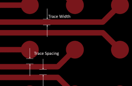
1. Trace Width and Spacing
Trace width determines how much current a trace can carry without overheating. For a standard 1 oz copper layer, a trace width of 10 mils (0.254 mm) can typically handle about 0.5 amps. Spacing, on the other hand, prevents electrical interference or short circuits between traces. A common rule is to keep at least 6 mils (0.152 mm) of spacing between traces for low-voltage designs.
2. Component Placement
Place components logically to minimize trace lengths and avoid clutter. For instance, keep high-speed components close to each other to reduce signal delays. Also, ensure heat-generating parts like power regulators have enough space for cooling, typically at least 0.5 inches (12.7 mm) from other components.
3. Power and Ground Planes
A solid ground plane helps reduce noise and provides a stable reference for signals. Ensure your power and ground traces are wide enough to handle the current—often at least 20 mils (0.508 mm) for small boards. Avoid routing signals over split planes, as this can cause interference.
4. Via Usage
Vias connect traces between layers, but too many can weaken the board. Use vias sparingly and ensure they’re at least 12 mils (0.305 mm) in diameter for standard designs. Also, keep vias away from high-speed signal paths to avoid signal distortion.
These basic rules are often turned into constraints within your design software, ensuring you follow them automatically as you work.
Introduction to Constraint Management: Key Concepts
Now that you understand some basic PCB design rules, let’s explore an introduction to constraint management. Constraints are essentially digital versions of design rules, enforced by your PCB design software to guide your layout and routing.
Types of Constraints in PCB Design
There are several types of constraints you’ll encounter in PCB design. Here are the most common ones for beginners:
- Physical Constraints: These include board size, component placement areas, and keep-out zones where no traces or parts can go. For example, you might set a keep-out zone of 0.2 inches (5 mm) around the board edge to avoid manufacturing issues.
- Electrical Constraints: These control signal behavior, such as impedance matching for high-speed traces (often targeting 50 ohms for RF designs) or maximum trace lengths to prevent delays.
- Manufacturing Constraints: These ensure your design can be built, such as minimum drill sizes for vias (typically 0.3 mm) or minimum trace widths for the chosen fabrication process.
- Thermal Constraints: These manage heat dissipation, like spacing requirements for power components or specifying copper pour areas for heat sinking.
How Constraint Management Works
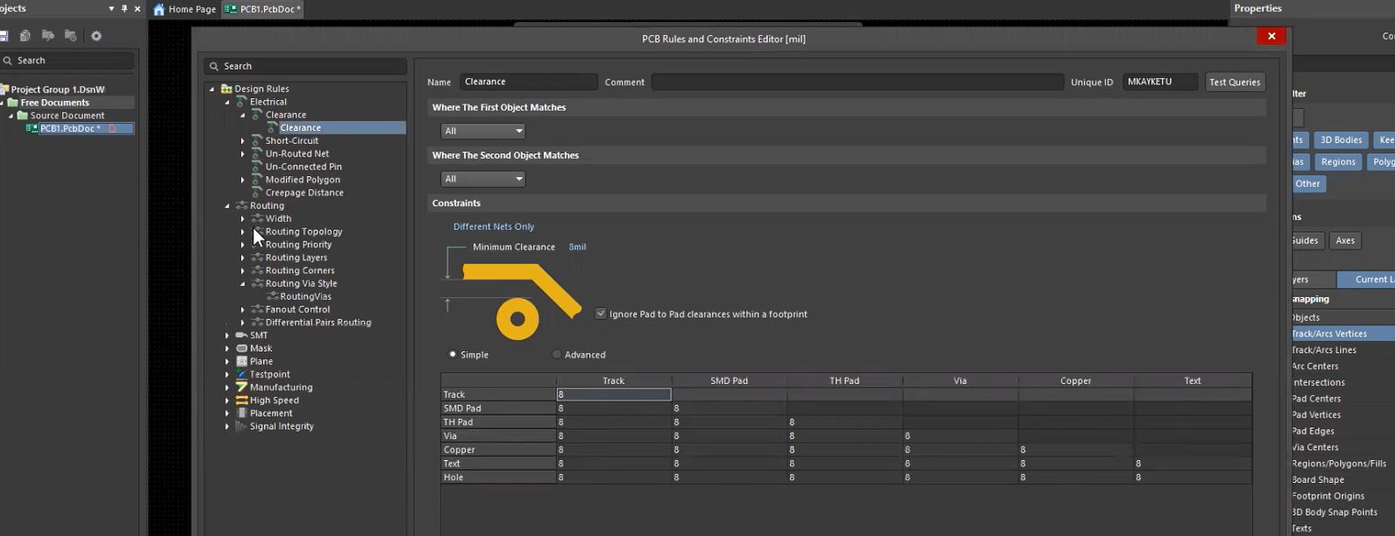
Constraint management starts with defining these rules in your design software. Once set, the software monitors your design in real-time, flagging any violations. For instance, if you set a minimum trace spacing of 6 mils and accidentally place two traces only 4 mils apart, the software will highlight the error. This immediate feedback helps beginners avoid mistakes and learn good design habits.
PCB Design Software Constraints: Tools for Beginners
Modern PCB design tools come with built-in features to manage PCB design software constraints. These tools make it easy to set and follow rules, even if you’re new to design. Here’s how you can use software to handle constraints effectively.
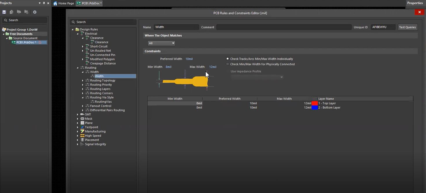
Setting Constraints in Software
Most design platforms have a dedicated constraints editor or panel where you can input rules. For example, you might set a rule that all traces carrying more than 1 amp must be at least 20 mils wide. Once entered, the software ensures your design adheres to this rule during layout and routing.
Design Rule Checks (DRC)
Design Rule Checks are automated processes in software that scan your design for constraint violations. Running a DRC before finalizing your design can catch issues like insufficient spacing or unconnected nets. For beginners, this feature is invaluable as it acts like a teacher pointing out mistakes.
Common Software Features for Constraints
Look for software with features like real-time error checking, customizable rule sets, and visual indicators for violations. These tools simplify constraint management and help you focus on creativity rather than worrying about errors.
Simple PCB Design Guidelines for Constraint Management
To wrap up, here are some simple PCB design guidelines to help you manage constraints effectively as a beginner. These tips will build a strong foundation for your designs.
1. Start with a Plan
Before setting constraints, plan your design by identifying key requirements. Will your board handle high-speed signals? Does it need to fit in a small enclosure? Answering these questions helps you define relevant constraints, like maximum trace lengths (e.g., under 100 mm for high-speed signals) or board dimensions (e.g., 50 mm x 50 mm).
2. Use Default Constraints as a Starting Point
Most design tools come with default constraint sets for common scenarios. Use these as a starting point and adjust them based on your project needs. For instance, if the default trace spacing is 8 mils but your manufacturer requires 10 mils, update the constraint accordingly.
3. Prioritize Critical Constraints
Focus on constraints that impact performance and manufacturability first. For example, set electrical constraints for signal integrity (like impedance of 50 ohms for RF traces) before worrying about less critical rules like aesthetic component alignment.
4. Test and Validate
After setting constraints, run a Design Rule Check and review any errors. Fix violations early to avoid bigger issues later. If your software supports simulation, use it to test signal behavior under your constraints, ensuring they’re realistic.
5. Learn from Each Project
Every PCB design teaches you something new about constraints. Keep notes on what worked and what didn’t. Over time, you’ll develop a personal set of rules that streamline your workflow.
Common Mistakes to Avoid in Constraint Management
As a beginner, it’s easy to make mistakes when managing constraints. Here are a few pitfalls to watch out for:
- Ignoring Manufacturing Limits: Always check your manufacturer’s capabilities. If they can’t produce traces thinner than 6 mils, setting a constraint for 4 mils will lead to production failures.
- Overloading Constraints: Setting too many or overly strict rules can make your design impossible to complete. Start with essential constraints and add more as needed.
- Forgetting to Update Rules: If your project changes (e.g., switching from a 2-layer to a 4-layer board), update your constraints to match the new setup.
Conclusion: Mastering Constraint Management as a Beginner
Constraint management is a vital skill for anyone starting in PCB design. By understanding PCB design constraints for beginners, following basic PCB design rules, and applying simple PCB design guidelines, you can create boards that are functional, reliable, and ready for manufacturing. Whether you’re just getting an introduction to constraint management or navigating PCB design software constraints, remember that constraints are your roadmap to success.
Start small, use the tools available in your design software, and build on each project. With practice, managing constraints will become second nature, allowing you to focus on creativity and innovation in your designs. At ALLPCB, we’re committed to supporting your journey with resources and expertise to help you succeed in every step of PCB design.