 ALLPCB


Introduction
Analog circuits demand precise signal integrity, where even minor noise can degrade performance in applications like sensors, amplifiers, and data acquisition systems. Component placement plays a critical role in analog PCB layout by determining how effectively noise and interference are contained. Engineers must prioritize strategies that isolate sensitive analog sections from digital noise sources, such as switching regulators or high-speed logic. Proper grounding analog circuits and shielding techniques analog PCB further enhance reliability. This article explores structured approaches to component placement for low noise, drawing on established engineering principles. By implementing these practices, designers achieve cleaner signals and robust system performance.
Noise in analog designs arises from electromagnetic interference, crosstalk, and ground bounce, all exacerbated by suboptimal layouts. Interference reduction analog design requires thoughtful positioning of components relative to power supplies, clocks, and I/O lines. Standards like IPC-2221 provide foundational guidelines for such layouts, emphasizing controlled impedance and minimized loop areas. The goal is to create a PCB environment where analog signals propagate with minimal distortion.
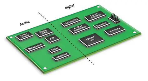
Why Component Placement Matters in Analog Circuits
Component placement influences every aspect of signal quality in analog PCB layout. Sensitive components, such as operational amplifiers or ADCs, must be positioned to avoid proximity to high-current paths or fast-switching elements. This separation reduces capacitive and inductive coupling that introduces noise. For instance, placing bypass capacitors close to IC pins minimizes high-frequency noise on power rails. Engineers benefit from systematic placement rules that align with physical principles of electromagnetic fields.
In mixed-signal boards, digital sections generate return currents that can corrupt analog grounds if not managed. Component placement for low noise involves grouping analog functions together, forming isolated islands. This partitioning prevents digital ground bounce from propagating into analog domains. Practical outcomes include improved signal-to-noise ratios and compliance with performance specs in IPC-6012. Ultimately, deliberate placement translates to fewer iterations during prototyping.
The economic impact is significant, as poor layouts lead to respins and delayed time-to-market. By contrast, optimized placement streamlines manufacturing and testing. Grounding analog circuits becomes more effective when components are clustered logically.
Key Noise Mechanisms in Analog PCB Design
Noise sources in analog circuits include thermal noise, shot noise, and externally induced interference. Crosstalk occurs when adjacent traces couple signals magnetically or capacitively, with coupling strength proportional to trace length and proximity. To mitigate this, maintain separation distances exceeding three times the trace width for critical signals. Ground loops form when multiple ground paths create voltage differentials, injecting hum or ripple into analog lines.
Electromagnetic interference from external fields couples into loops formed by signal returns. Larger loop areas act as antennas, amplifying pickup at frequencies like 50/60 Hz or RF bands. Component placement directly controls these loop geometries by dictating trace routings. Power supply noise, often from SMPS ripple, travels through shared planes unless isolated.
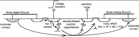
Return path discontinuities cause impedance mismatches, leading to reflections and ringing. In high-impedance analog nodes, even microvolts of noise can swamp signals. Understanding these mechanisms guides placement decisions, ensuring low-inductance paths for returns.
Related Reading: Optimizing Op-Amp PCB Layout for EMI Reduction in Sensitive Analog Circuits
Best Practices for Analog PCB Layout and Component Placement
Start with board partitioning to separate analog, digital, and power sections physically. Place analog components in a dedicated zone, away from board edges exposed to chassis EMI. Orient sensitive components to minimize trace lengths, such as positioning feedback resistors near op-amp pins. Decoupling capacitors should sit within 5 mm of power pins to shunt noise effectively.
For component placement for low noise, prioritize high-gain stages centrally, shielded by lower-gain buffers. Avoid placing inductors or transformers near amplifiers, as their fields induce offsets. Use via fencing around analog areas to stitch ground planes, reducing slot radiation. These steps form the backbone of interference reduction analog design.
Routing complements placement by keeping analog traces short and shielded. Differential pairs require symmetric lengths to balance common-mode rejection.
Related Reading: Mastering Analog PCB Layout: Component Placement for Signal Clarity
Grounding Analog Circuits: Strategies and Implementation
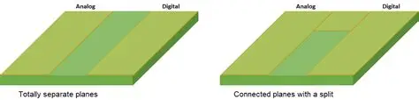
Grounding analog circuits requires distinct planes or partitions to prevent digital currents from contaminating analog references. Implement a single-point star ground for low-frequency analog, converging all returns at one node. For multilayer boards, dedicate inner layers to solid analog ground planes, connected via multiple vias.
Split-plane techniques isolate sections, with analog ground tied to the cleanest reference. Avoid routing signals over plane splits to prevent impedance jumps. J-STD-001 guidelines support these practices by specifying soldering integrity for low-noise connections. Bridge splits only under controlled conditions, like with 0-ohm jumpers.
Guard rings around op-amps channel leakage currents away from inputs. Monitor ground potential differences during layout review to ensure less than 1 mV drop.
Shielding Techniques for Analog PCB
Shielding techniques analog PCB include ground pours, guard traces, and moats. Enclose sensitive traces with grounded copper fills on adjacent layers, minimizing field fringing. Guard traces, biased at signal common, absorb common-mode noise without loading the circuit.
Moats etched in ground planes interrupt unwanted currents, but require careful bridging for returns. For RF analog, top-metal shields overpass sensitive lines. These methods reduce radiated susceptibility.
Component cans or enclosures provide ultimate shielding for ultra-sensitive nodes.
Advanced Placement Techniques for Interference Reduction
In high-density boards, use BGA placement with analog sections offset from digital cores. Floorplanning tools help visualize noise budgets during initial placement. Simulate parasitics post-placement to quantify coupling.
For precision analog, thermal management influences noise via Johnson noise variation. Place heat sources away from sensors. Iterative refinement, guided by IPC-2221 principles, yields optimal results.
Optocouplers or transformers isolate grounds in extreme cases.
Troubleshooting Common Placement Pitfalls
Overlooking bypass placement injects supply noise into signals. Solution: enforce proximity rules in design rules. Crystal oscillators near ADCs cause spurs; relocate with shielding.
Unbalanced differential pairs degrade CMRR; match lengths precisely. Review via counts under grounds to avoid inductance.
Post-layout EMI scans reveal issues early.
Conclusion
Effective component placement for low noise defines successful analog PCB layout. By partitioning sections, optimizing grounding analog circuits, and applying shielding techniques analog PCB, engineers minimize noise and interference. These practices ensure reliable performance across applications. Adhering to structured guidelines reduces risks and enhances design efficiency. Prioritize simulation and review for best outcomes.
FAQs
Q1: What are the primary considerations for analog PCB layout in mixed-signal designs?
A1: Analog PCB layout requires strict partitioning of analog and digital sections to prevent crosstalk and ground bounce. Place sensitive components like ADCs away from clocks and power switches. Use dedicated ground planes and guard traces for isolation. Component placement for low noise ensures short analog paths and effective decoupling. Follow these to achieve high signal integrity.
Q2: How does grounding analog circuits impact overall noise performance?
A2: Grounding analog circuits with split planes or star points isolates return currents from digital noise. This prevents voltage gradients that couple into signals. Multiple vias connect planes at low inductance. Shielding techniques analog PCB complement grounding for comprehensive protection. Proper implementation boosts SNR by orders of magnitude.
Q3: What shielding techniques analog PCB are most effective for interference reduction?
A3: Shielding techniques analog PCB include guard traces, ground pours, and moats around sensitive areas. These absorb stray fields and channel leakage currents. Enclose traces between ground layers for Faraday cage effects. Combine with component placement for low noise to minimize loop areas. Results show reduced EMI susceptibility.
Q4: Why is component placement critical for interference reduction analog design?
A4: Component placement for low noise controls coupling paths and loop geometries in analog designs. Sensitive amps near noise sources pick up offsets; separation mitigates this. Logical grouping simplifies shielding and grounding. Interference reduction analog design relies on this foundation for clean signals.
References
IPC-2221B - Generic Standard on Printed Board Design. IPC, 2003
IPC-6012E - Qualification and Performance Specification for Rigid Printed Boards. IPC, 2017
J-STD-001H - Requirements for Soldered Electrical and Electronic Assemblies. IPC, 2018


