 ALLPCB


In high-power applications, PCB thickness directly influences current-carrying capacity, heat dissipation, and long-term mechanical stability. Engineers working on power supplies, motor drives, and renewable energy systems must balance electrical performance with thermal and structural requirements. Standard board thicknesses often prove insufficient when currents exceed several amperes or when localized heating becomes a concern. Proper thickness selection reduces voltage drop, minimizes temperature rise, and helps maintain signal integrity in mixed-signal designs. This guide examines the engineering factors that determine suitable PCB thickness for demanding power environments.
Why PCB Thickness Matters in High-Power Designs
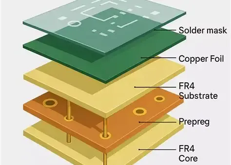
PCB thickness refers to the total stack-up dimension from the outer copper surface on one side to the outer copper surface on the opposite side. In power PCB design, this dimension affects trace resistance, thermal spreading, and the board’s ability to withstand mechanical stress during operation and assembly. Thicker boards provide greater copper cross-sectional area when combined with heavier copper weights, allowing higher current without excessive heating. Conversely, overly thick constructions can increase material cost, complicate drilling processes, and raise the risk of warpage during reflow. Industry standards such as IPC-6012E establish qualification requirements that help ensure boards meet performance expectations across varying thicknesses.
High-current PCB applications frequently involve continuous currents above 10 A or pulsed loads that generate significant I2R losses. In these cases, insufficient thickness leads to elevated trace temperatures that can degrade dielectric materials or cause delamination. Thermal considerations become especially important when components such as MOSFETs or IGBTs dissipate several watts each. Adequate board thickness supports better heat conduction away from hot spots toward heatsinks or chassis mounting points. Designers therefore evaluate thickness early in the layout phase rather than treating it as a secondary manufacturing detail.
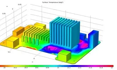
Dielectric material selection interacts with thickness choices. Higher glass-transition temperature materials tolerate greater heat but may require adjusted lamination cycles for thicker constructions. Thermal conductivity of the dielectric becomes relevant when power planes occupy inner layers and must conduct heat to outer surfaces. Designers often model these interactions using finite-element thermal analysis to predict steady-state temperatures under worst-case load conditions.
Technical Principles Governing Thickness Selection
Copper thickness, expressed in ounces per square foot, combines with overall board thickness to determine current-carrying capability. A 1 oz copper layer on a 1.6 mm board offers a baseline, while 2 oz or 3 oz copper on 2.0 mm or 2.4 mm substrates provides substantially more cross-sectional area for the same trace width. This relationship follows principles outlined in current-carrying capacity guidelines, where thicker copper and greater overall board thickness both contribute to lower resistance per unit length. Heat generated within traces spreads laterally through the copper planes and vertically through the dielectric, making total thickness a key variable in thermal resistance calculations.
Mechanical considerations also scale with thickness. Thicker boards exhibit higher flexural rigidity, which reduces flexing under vibration or during handling. This rigidity helps maintain solder joint integrity in high-power assemblies subjected to thermal cycling. At the same time, excessive thickness can increase the distance between layers, affecting controlled-impedance routing when high-speed signals coexist with power traces. Warpage tendencies during thermal excursions must be evaluated, because asymmetric copper distribution or uneven heating can distort the board enough to cause assembly defects.
Practical Guidelines for Selecting Thickness
Begin by determining maximum continuous and peak current requirements for each power net. Trace width calculators based on IPC-2152 provide starting points, after which overall board thickness and copper weight are adjusted to achieve acceptable temperature rise, typically limited to 10–20 °C above ambient. For currents exceeding 20 A, 2 oz or heavier copper combined with board thicknesses of 2.0 mm or greater frequently becomes necessary. When space constraints limit trace width, increasing copper weight or board thickness offers an alternative route to higher current capacity without widening conductors.
Thermal vias placed under power components help transfer heat to inner planes or opposite-side copper areas. Their effectiveness improves when the board thickness remains moderate, because longer via barrels increase thermal resistance. In very thick boards, designers may add additional vias or use filled vias to maintain heat flow. Copper planes should be sized generously and connected with multiple vias to avoid current crowding and localized heating.
Mechanical mounting points and connector locations influence thickness decisions. Boards that bolt to heatsinks or enclosures benefit from greater thickness to resist bowing under clamping forces. Conversely, designs that must remain lightweight may employ selective thickening only in high-current regions through embedded copper or stepped constructions. Fabrication capabilities should be reviewed early, because drilling aspect ratios and plating uniformity become more challenging as thickness increases.
Best Practices and Verification Steps
Prototype boards should undergo thermal imaging under representative load conditions to validate thickness choices. Measured temperature rises can be compared against simulation results and adjusted if necessary by increasing copper weight or adding thermal relief modifications. Electrical testing confirms that voltage drop remains within acceptable limits across the full current range. Mechanical inspection includes checks for warpage after thermal cycling to ensure compliance with flatness requirements.
Documentation of the stack-up, including exact dielectric thicknesses and copper weights, supports consistent manufacturing outcomes. When multiple suppliers are involved, clear specification of overall thickness tolerance prevents unexpected variations that could affect thermal or mechanical performance. Regular review of IPC-A-600K acceptability criteria helps maintain quality across production lots.

Conclusion
Selecting PCB thickness for high-power applications requires simultaneous consideration of current capacity, thermal performance, and mechanical stability. Thicker boards paired with heavier copper weights address high-current demands while supporting effective heat spreading. Structured evaluation using established guidelines, followed by prototype verification, yields designs that operate reliably under demanding conditions. Early collaboration between electrical, thermal, and manufacturing teams reduces the likelihood of costly redesigns.
FAQs
Q1: What PCB thickness is typically recommended for high-current PCB designs?
A1: Thickness selection depends on current levels, copper weight, and allowable temperature rise. Boards carrying more than 10–20 A often use 2.0 mm or greater overall thickness combined with 2 oz or heavier copper to maintain acceptable heating and mechanical strength.
Q2: How do PCB thermal considerations change with increased board thickness?
A2: Greater thickness improves lateral heat spreading through copper planes but can lengthen thermal paths through vias. Designers balance these effects by optimizing via placement and copper distribution to keep component temperatures within limits.
Q3: When should heavy copper PCB constructions be considered over standard thickness?
A3: Heavy copper becomes advantageous when trace widths are constrained by layout density yet current demands remain high. The additional copper cross-section allows narrower traces to carry the required load without excessive voltage drop or heating.
Q4: Does increasing PCB thickness affect high-power assembly processes?
A4: Thicker boards require attention to drilling aspect ratios, plating uniformity, and reflow profiles to avoid warpage or incomplete solder joints. Proper process adjustments ensure reliable assembly outcomes across varying thicknesses.
References
IPC-6012E — Qualification and Performance Specification for Rigid Printed Boards. IPC, 2017
IPC-2152 — Standard for Determining Current Carrying Capacity in Printed Board Design. IPC, 2009
IPC-A-600K — Acceptability of Printed Boards. IPC, 2020


