 ALLPCB


What Is BGA Fanout and Why It Matters
BGA packages enable high pin counts in compact footprints, making them essential in modern electronics. Fanout refers to the process of routing signals from the array of solder balls to the outer layers or inner traces of the printed circuit board. Effective fanout directly influences board density, manufacturability, and electrical performance. Designers must balance space constraints with requirements for signal integrity and thermal management. Poor fanout choices can lead to increased layer counts or routing congestion in subsequent stages of layout.
BGA fanout encompasses the initial escape routing that connects each ball to a via or trace. This step occurs immediately beneath the component footprint and sets the foundation for the rest of the interconnect network. In high-density designs, fanout determines whether additional layers become necessary and how effectively power and ground returns can be placed. Industry standards such as IPC-6012E guide the qualification of rigid boards that must accommodate these dense interconnects. When fanout is executed well, it supports higher component placement density without compromising assembly yield or long-term reliability.
Technical Principles of BGA Fanout
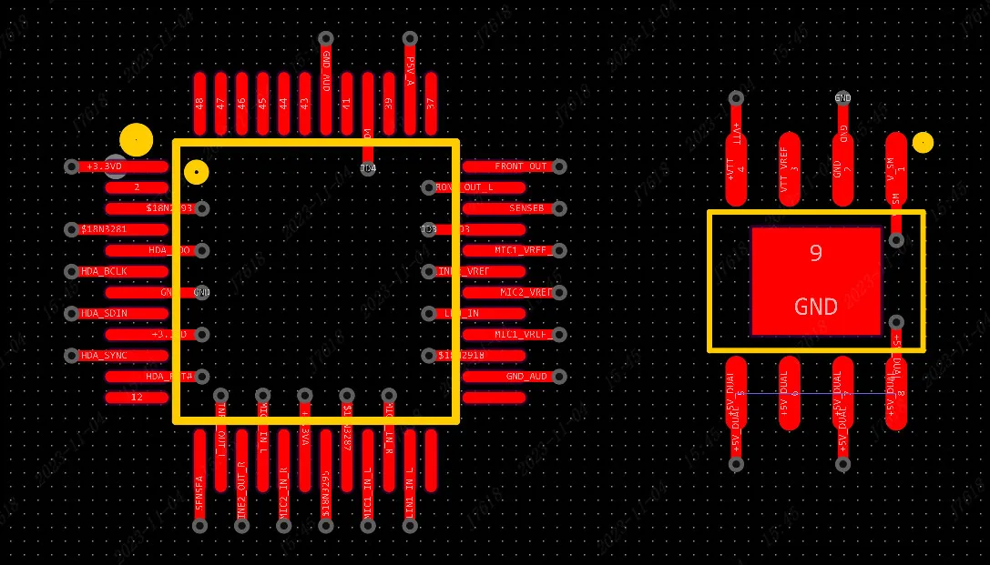
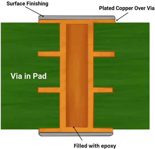
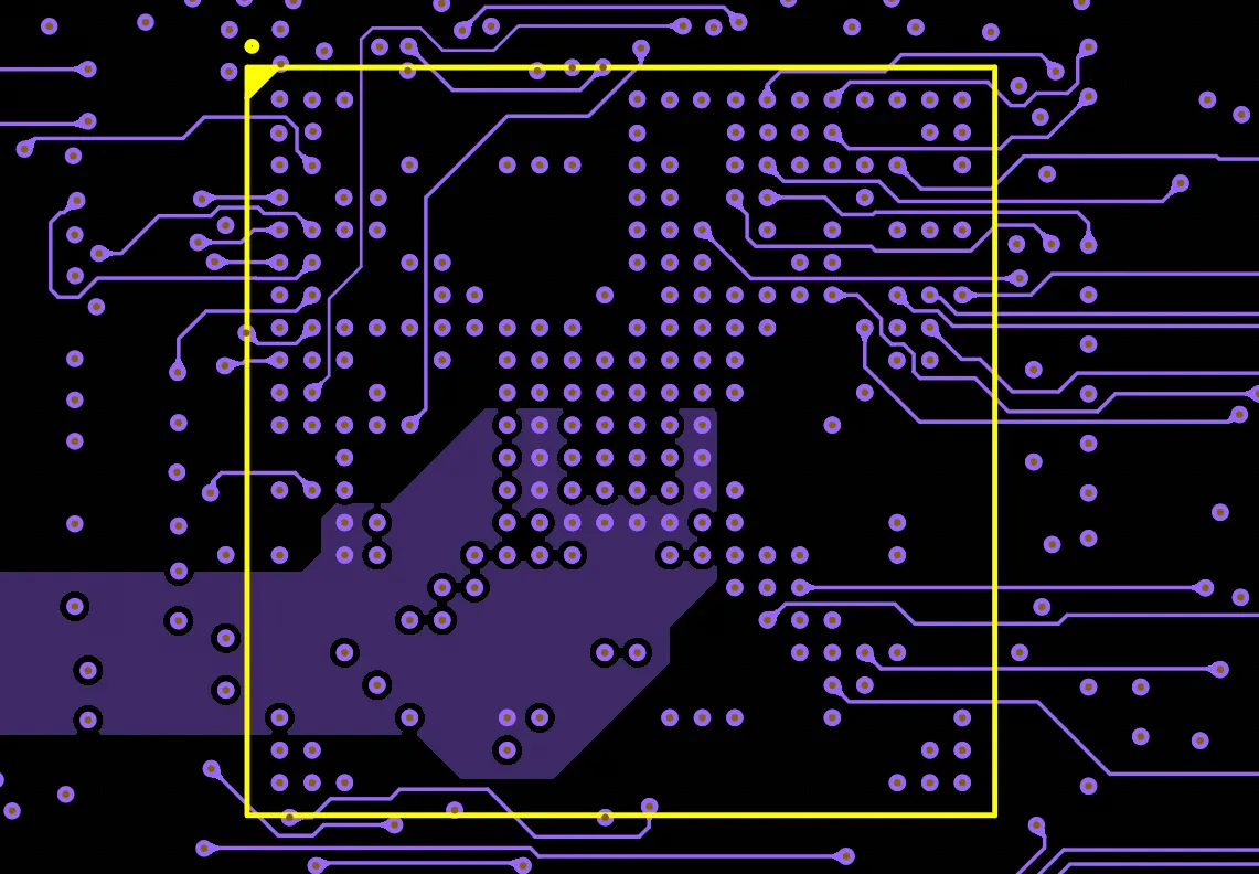
The mechanism begins with the ball pitch, which dictates the available real estate for traces and vias. Designers typically employ dog-bone patterns or direct via-in-pad approaches to escape signals from inner balls. Via placement must avoid excessive stub lengths that create reflections and degrade high-speed signals. Signal integrity considerations include controlling impedance along the fanout path and minimizing crosstalk between adjacent traces. Impedance control becomes critical when differential pairs or controlled-impedance nets exit the array. Via-in-pad technology reduces the distance signals travel before reaching inner layers, yet it introduces challenges related to via fill and planarization during fabrication.
Thermal expansion differences between the package and board also influence via and trace placement. Proper fanout strategies distribute current return paths evenly to maintain low inductance. Structured engineering analysis shows that staggered via arrangements often provide better routing channels than inline patterns in fine-pitch BGAs. These choices affect both the immediate electrical performance and the overall stack-up decisions for the board.
BGA Fanout Design Rules and Strategies
Design rules for BGA fanout typically specify minimum trace widths, clearances, and via diameters based on the chosen fabrication process. A common strategy involves prioritizing power and ground connections first, followed by high-speed differential pairs. Via placement should maintain consistent spacing to support controlled impedance while leaving adequate channels for subsequent routing. When signal integrity requirements are stringent, designers evaluate via stub length and consider back-drilling or blind vias to shorten discontinuities.
Impedance control in fanout demands careful selection of dielectric thickness and trace geometry. Differential pair routing within the fanout region requires matched lengths and symmetric reference planes. Practical layouts often combine multiple via technologies to optimize both density and performance. These decisions follow logical sequencing that begins with package-specific ball maps and proceeds outward.
BGA Fanout Signal Integrity and Impedance Control
Signal integrity during fanout depends on maintaining consistent return paths and minimizing discontinuities. Impedance mismatches at via transitions can cause reflections that affect eye diagrams at multi-gigabit speeds. Designers calculate target impedance values early and verify them through stack-up modeling before committing to final via locations. Crosstalk is mitigated by increasing spacing or inserting ground vias between critical nets.
BGA fanout impedance control also involves selecting appropriate via aspect ratios and pad sizes. Reference planes must remain continuous beneath the fanout region to support proper current return. When these principles are applied consistently, the resulting interconnect exhibits predictable electrical behavior across temperature and frequency ranges. Standards such as JEDEC J-STD-020E address moisture sensitivity considerations that indirectly affect via and pad reliability after reflow.
Practical Best Practices for Via Placement in BGA Fanout
Via placement strategies prioritize escape efficiency while preserving routing resources on inner layers. Placing vias directly under balls reduces trace length but requires reliable via fill processes. Staggered or offset via grids create additional routing channels between rows. Designers review the entire escape pattern for symmetry to balance mechanical stress across the package footprint.
Power distribution benefits from multiple vias per ball to lower inductance. Ground vias should be located close to signal vias to maintain tight coupling. These practices reduce the risk of electromagnetic interference and improve overall board performance. Iterative review of the fanout pattern against manufacturing tolerances ensures the design remains producible.
Conclusion
BGA fanout forms the critical first step in realizing the full potential of high-pin-count packages. Logical application of design rules, attention to signal integrity, and strategic via placement yield boards that meet both electrical and manufacturing requirements. Consistent reference to established industry standards supports repeatable results across projects. Designers who master these fundamentals reduce iteration cycles and improve time-to-market for complex assemblies.
FAQs
Q1: What are the primary BGA fanout design rules that ensure reliable routing?
A1: Key BGA fanout design rules address minimum trace width, clearance, via diameter, and spacing relative to ball pitch. These rules also cover via stub length limits and impedance targets for high-speed nets. Following them systematically prevents congestion and supports subsequent routing layers.
Q2: How do different BGA fanout strategies affect signal integrity?
A2: BGA fanout strategies such as dog-bone versus via-in-pad influence stub length and transition discontinuities. Shorter paths generally improve signal integrity by reducing reflections. Proper reference plane continuity and via placement further minimize crosstalk and maintain target impedance.
Q3: Why is impedance control important during BGA fanout?
A3: BGA fanout impedance control ensures that signals encounter consistent characteristic impedance from the ball through the initial via and trace. Mismatches in this region can degrade rise times and increase bit error rates. Careful geometry selection and stack-up planning achieve the required control.
Q4: What considerations guide via placement in BGA fanout layouts?
A4: Via placement in BGA fanout balances escape density, mechanical reliability, and electrical performance. Factors include current-carrying needs, thermal paths, and avoidance of excessive stress concentrations. Staggered arrangements often optimize channel availability for inner-layer routing.


