 ALLPCB


Introduction
High-speed electronic systems increasingly rely on complex multilayer boards to accommodate dense routing and multiple signal layers. In a 14-layer PCB, the stackup provides ample space for power planes, ground planes, and signal traces, yet it also introduces challenges for via structures. Backdrilling addresses one of the most common sources of signal degradation by removing the unused portion of plated through-hole vias. Engineers apply this technique when operating frequencies exceed several gigahertz and when via stubs would otherwise create reflections that distort waveforms. The process improves overall signal integrity without requiring a complete redesign of the board stackup. Proper implementation demands close coordination between layout and fabrication teams to maintain mechanical integrity and electrical performance.
What Is Backdrilling and Why It Matters
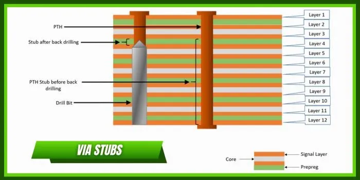
Backdrilling removes the copper plating from the non-functional segment of a via after the board has been drilled and plated. This segment, known as the via stub, extends beyond the last layer that the signal actually uses and acts as an open stub transmission line. In 14-layer PCB backdrilling applications, the stub length can reach several millimeters, producing significant impedance discontinuities at high data rates. The technique therefore becomes essential for maintaining clean eye diagrams and meeting bit-error-rate targets in serial links such as PCIe, 100 Gigabit Ethernet, and high-speed memory interfaces. Without backdrilling, reflections from the stub can couple into adjacent traces and degrade timing margins across the entire system. Industry practice shows that boards operating above 5 Gbps per lane benefit measurably when stub lengths are reduced below 0.5 mm. The approach also supports denser via placement because designers no longer need to avoid long stubs by shifting signals to outer layers.
Technical Principles and Signal Integrity Mechanisms
A plated through-hole via in a 14-layer stackup creates a continuous conductive path from the top to the bottom of the board. When a signal transitions only between layers 3 and 10, for example, the remaining via segment from layer 10 to layer 14 remains electrically connected and functions as a quarter-wave resonator at certain frequencies. This resonance produces return loss peaks and group-delay variation that directly impair signal integrity. Backdrilling severs the stub at a controlled depth, converting the via into a shorter transmission-line segment whose impedance more closely matches the surrounding traces. The resulting reduction in reflection coefficient improves insertion loss and reduces crosstalk, particularly when multiple high-speed nets share the same via field. Engineers quantify the improvement using time-domain reflectometry and frequency-domain S-parameter measurements before and after the backdrill operation. Thermal and mechanical stresses introduced by the secondary drilling step must remain within limits defined by board material properties to avoid delamination or barrel cracking.
Practical Solutions and Best Practices in High-Speed Design
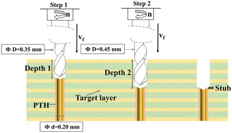
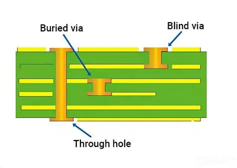
Designers begin by identifying all high-speed nets whose via transitions leave stubs longer than one-tenth of the signal wavelength at the highest frequency of interest. They then specify backdrill depths on the fabrication drawing with tolerances typically held to plus or minus 0.1 mm. Controlled-depth drilling requires accurate registration between the primary and secondary drill operations, which is achieved through fiducial alignment and X-ray verification on the production floor. Alternative via structures such as blind or buried vias can eliminate stubs entirely but increase fabrication cost and limit layer-pair flexibility in a 14-layer PCB. When backdrilling is selected, engineers also review via pad and antipad dimensions to ensure adequate clearance after the secondary drill removes plating. Post-backdrill inspection includes cross-section analysis to confirm that the remaining via barrel maintains at least the minimum copper thickness required for current-carrying capacity. Simulation tools model the shortened via as a lumped element or full-wave structure to predict the final S-parameters before committing to fabrication.
Manufacturing and Quality Considerations for 14-Layer Boards
Fabrication of backdrilled 14-layer PCBs follows the same lamination and plating sequences used for standard boards until the final drilling stage. The secondary drill bit must enter from the side opposite the functional via segment to avoid damaging active circuitry. Depth control is verified on test coupons that replicate the production stackup, ensuring the drill stops within the target dielectric layer. Boards are then subjected to electrical testing that includes continuity, isolation, and impedance measurements on representative traces. Thermal cycling and interconnect stress testing confirm that the backdrilled vias retain mechanical integrity under expected operating conditions. Documentation of drill programs and inspection results supports traceability required for high-reliability applications.
Conclusion
Backdrilling provides a practical and widely adopted method for mitigating via-stub effects in 14-layer PCB designs that carry high-speed signals. By shortening the unused via segment, engineers reduce reflections, improve return loss, and maintain timing margins without resorting to more expensive via structures. Successful implementation requires precise depth control, thorough simulation, and adherence to established fabrication practices. When applied consistently, the technique supports reliable operation of complex electronic systems while preserving the routing density advantages of thick multilayer boards.
FAQs
Q1: What is 14-layer PCB backdrilling and how does it improve signal integrity?
A1: Backdrilling removes the unused lower portion of a plated through-hole via after initial fabrication. In a 14-layer PCB this shortens the via stub that would otherwise act as a reflective transmission-line segment. The reduction in stub length lowers return loss and crosstalk, allowing high-speed signals to maintain cleaner waveforms and better timing margins.
Q2: When should designers consider backdrilling for high-speed PCB design?
A2: Designers evaluate backdrilling whenever via transitions on high-speed nets leave stubs longer than approximately one-tenth of the wavelength at the maximum operating frequency. This situation commonly arises in 14-layer boards carrying multi-gigabit serial links. Early identification during layout allows specification of backdrill depths on fabrication drawings and avoids costly respins.
Q3: How does reducing via stubs affect overall board performance?
A3: Shorter via stubs decrease impedance discontinuities and quarter-wave resonances that distort signals. The result is lower insertion loss, improved eye opening, and reduced coupling to neighboring nets. In 14-layer PCB backdrilling projects these electrical benefits are achieved while retaining the mechanical strength of the full board thickness.
Q4: What design practices support effective via optimization in multilayer boards?
A4: Engineers map all high-speed net transitions early and compare stub lengths against frequency-dependent limits. They coordinate backdrill depths with fabricators, verify registration accuracy, and validate performance through simulation and measurement. These steps ensure that via optimization contributes to overall signal integrity without introducing new mechanical risks.
References
IPC-6012E — Qualification and Performance Specification for Rigid Printed Boards. IPC, 2017
IPC-A-600K — Acceptability of Printed Boards. IPC, 2020
IPC-2221B — Generic Standard on Printed Board Design. IPC, 2012


