 ALLPCB


Introduction
Ball Grid Array (BGA) components present unique demands in surface mount technology assembly due to their dense array of solder balls and fine pitches. Effective BGA stencil design ensures precise solder paste deposition, which is critical for forming reliable interconnections during reflow soldering. Engineers often face BGA soldering challenges such as insufficient paste volume leading to opens or excess causing bridges. Advanced techniques focus on optimizing aperture size for BGA pads, controlling solder paste volume for BGA applications, and selecting appropriate stencil thickness for BGA components. These methods draw from established guidelines to enhance yield and minimize defects. Mastering these approaches allows for consistent performance in high-density boards.
Understanding BGA Stencil Design and Its Importance
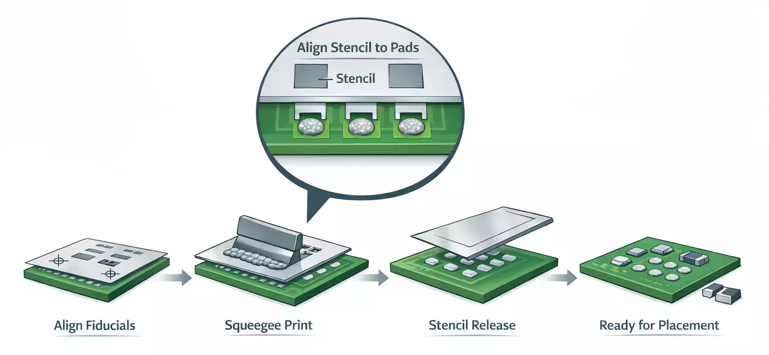
BGA stencil design involves creating precise apertures in a thin metal foil that aligns with the PCB pads under the BGA footprint. The stencil acts as a template to deposit a controlled amount of solder paste, which later reflows to form joints with the component's balls. Proper design directly influences solder paste volume for BGA, preventing issues like voids or non-wets. In high-volume production, suboptimal designs amplify BGA soldering challenges, resulting in rework costs and reliability failures. According to IPC-7525C guidelines, key parameters include aperture geometry and foil thickness to achieve consistent transfer efficiency. This foundational step sets the stage for robust assembly processes.
The relevance stems from the evolution of BGA pitches down to 0.4mm or finer, demanding tighter tolerances. Engineers must balance paste release with volume control to match the collapsed ball height post-reflow. Poor stencil design exacerbates challenges like head-in-pillow defects, where paste height mismatches the ball. Optimizing BGA stencil design thus supports higher assembly yields and long-term joint integrity.
Technical Principles Behind Effective BGA Stencils
The core principle in BGA stencil design revolves around the area ratio, defined as the open aperture area divided by the sidewall area. IPC-7525C recommends maintaining an area ratio above 0.66 to ensure reliable solder paste release, particularly for circular apertures common in BGA pads. For finer pitches, transitioning from round to slightly squared apertures improves paste flow without compromising volume. Aperture size for BGA typically scales with pad diameter, often at 1:1 for pitches over 1.0mm or reduced by 5-20% for tighter arrays to control solder paste volume for BGA. These adjustments prevent bridging between adjacent balls during printing and reflow.
Stencil thickness for BGA influences both paste volume and printability. Thinner foils, around 0.10 to 0.15mm, suit fine-pitch BGAs by promoting better release, while thicker ones provide more volume for larger pitches. The aspect ratio, aperture width over thickness, should exceed 1.5 to avoid paste retention in walls. Engineers calculate volume as aperture area times thickness times transfer efficiency, typically 75-90% for laser-cut stencils. Surface tension and powder particle size in the paste interact with these dimensions, affecting slump and release.
Powder type per J-STD-005 classification plays a role, with finer Types 4 or 5 enabling smaller apertures without clogging. Wall finish from manufacturing, such as electro-polishing, reduces friction for cleaner release. These mechanisms ensure the deposited paste bridges effectively with BGA balls during placement and reflow.
Related Reading: Advanced Stencil Design Techniques for QFN and BGA Components
Best Practices for Optimizing Solder Paste Volume and Aperture Design
Start with pitch-specific aperture sizing in BGA stencil design. For 0.8mm pitch, use round apertures at full pad size; for 0.5mm, reduce by 10-15% or adopt home-plate shapes to enhance volume control. Verify designs via simulation or SPI (solder paste inspection) to confirm solder paste volume for BGA stays within 100-125% of target. Step stencils allow varying thickness across the board, thinner for BGA areas and thicker elsewhere.
Select stencil thickness for BGA based on the smallest aperture: 0.125mm suits most fine-pitch while balancing volume. Employ nano-coatings to boost release efficiency up to 95%, reducing variability. Print parameters like squeegee pressure and speed fine-tune deposition; lower speeds aid fine features.
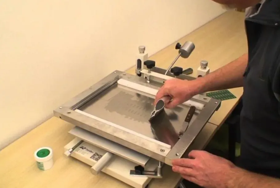
Incorporate keep-out zones of at least 0.89mm between fine-pitch apertures to prevent smearing. Validate with test prints, adjusting for paste rheology. These practices mitigate common defects and align with IPC-7095 recommendations for BGA assembly.
Overcoming BGA Soldering Challenges Through Stencil Techniques
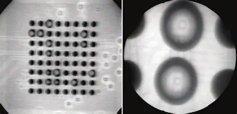
BGA soldering challenges often trace to inconsistent solder paste volume for BGA, leading to voids or incomplete collapses. Head-in-pillow occurs when paste height exceeds ball stand-off, causing misalignment; counter this by precise aperture size for BGA reductions. Bridging plagues fine pitches, resolved via optimized area ratios and trapezoidal walls from laser cutting.
Warpage mismatches between BGA and PCB exacerbate issues; use low-volume paste strategically to allow self-alignment during reflow. Tombstoning is rare but possible in mixed assemblies; uniform stencil thickness for BGA prevents it. Troubleshooting involves X-ray analysis post-reflow to correlate defects with print data.
Advanced troubleshooting employs DOE (design of experiments) varying aperture size for BGA and thickness. Profile optimization per JEDEC J-STD-020 complements stencil tweaks for moisture-sensitive devices.
Related Reading: Troubleshooting Common BGA Rework Defects: A Practical Guide
Conclusion
Advanced BGA stencil design techniques center on precise control of aperture size for BGA, solder paste volume for BGA, and stencil thickness for BGA to conquer soldering challenges. Adhering to principles like area ratio thresholds ensures reliable paste transfer and joint formation. Practical implementation through pitch-tailored apertures and process validation yields robust assemblies. Engineers benefit from these methods in achieving high yields and durability. Continuous refinement based on inspection data sustains performance in evolving fine-pitch applications.
FAQs
Q1: What is the ideal aperture size for BGA in stencil design?
A1: Aperture size for BGA depends on pitch: use 1:1 round apertures for >1.0mm pitches and 80-95% reductions for 0.5-0.8mm to control solder paste volume for BGA. This prevents bridging while ensuring sufficient height for reflow collapse. IPC-7525C area ratio >0.66 guides consistent release. Validate with SPI for uniformity.
Q2: How does stencil thickness for BGA affect solder paste volume?
A2: Stencil thickness for BGA typically ranges 0.10-0.15mm for fine pitches, directly scaling paste volume as area times thickness times efficiency. Thinner foils enhance release for small apertures but reduce volume; balance via step stencils. This addresses BGA soldering challenges like voids from low volume or bridges from excess.
Q3: What are common BGA soldering challenges related to stencils?
A3: BGA soldering challenges include voids, head-in-pillow, and bridging from poor BGA stencil design. Insufficient solder paste volume for BGA causes opens, while excess leads to shorts. Optimize aperture size for BGA and thickness per IPC guidelines. Process controls like print speed mitigate variability.
Q4: How to optimize solder paste volume for BGA assemblies?
A4: Target 75-125% transfer efficiency by selecting Type 4/5 paste and nano-coated stencils. Adjust aperture size for BGA to match ball collapse needs, verifying with volume calculations. Address BGA soldering challenges through SPI and reflow profiling. Consistent practices per J-STD-005 ensure reliability.


