 ALLPCB


Robotics systems demand compact, reliable electronics that handle complex signal routing, power distribution, and thermal loads within tight mechanical envelopes. Advanced layout methods address these constraints by increasing routing density while preserving electrical performance and mechanical integrity. Multi-layer PCB design forms the foundation for such applications, allowing separate planes for power, ground, and signals. High-density interconnect (HDI) techniques further reduce board size without sacrificing functionality. Blind and buried vias, along with via-in-pad constructions, eliminate wasted space and improve component placement flexibility. These approaches align with the needs of motion control, sensor fusion, and embedded processing modules common in robotic platforms.
Why Advanced PCB Techniques Matter in Robotics
Space limitations in robotic arms, mobile bases, and end-effectors require boards that pack more circuitry into smaller footprints. Multi-layer PCB design supports this by stacking conductive layers separated by insulating dielectrics, enabling shorter interconnects and better impedance control. High-density interconnect (HDI) extends this capability through finer features and microvia structures that connect only selected layers. In robotic environments, vibration, temperature cycling, and electromagnetic interference further emphasize the value of these methods for maintaining signal integrity over extended operation. Designers therefore prioritize techniques that reduce via stubs, minimize board thickness, and optimize thermal paths while meeting mechanical durability requirements.
Technical Principles of Multi-Layer PCB Design
A multi-layer PCB consists of alternating copper and dielectric layers laminated under heat and pressure. Inner layers typically carry power and ground planes that provide low-impedance return paths and shielding for sensitive signals on outer layers. Controlled impedance routing becomes feasible when reference planes sit adjacent to signal traces, reducing crosstalk and reflections that could disrupt motor drivers or encoder interfaces. Layer stackup symmetry helps control warpage during thermal excursions encountered in robotic duty cycles. Sequential lamination processes allow precise registration of fine features across multiple layers, supporting the dense interconnect patterns required for processor-to-peripheral communication.
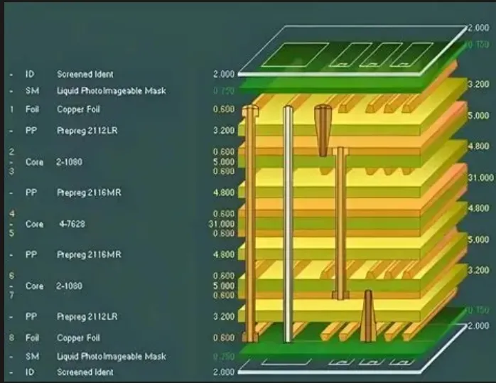
Blind and Buried Vias in High-Density Layouts
Blind vias connect an outer layer to one or more inner layers without penetrating the full board thickness. Buried vias link only inner layers, remaining invisible from both surfaces. These constructions remove the stub portion of a conventional through-hole via, lowering parasitic inductance and capacitance that degrade high-speed signals in robotic communication buses. By freeing surface real estate, blind and buried vias allow components to sit closer together and permit routing on layers that would otherwise be blocked. Fabrication involves sequential drilling and plating steps that must maintain alignment tolerances to avoid yield loss. The resulting interconnect density supports the compact controller boards used in collaborative robots and autonomous mobile platforms.
Via-in-Pad Technology and Its Advantages
Via-in-pad places a via directly beneath a component land, typically under a ball-grid-array or land-grid-array package. This eliminates the need for fan-out traces on the surface layer, shortening signal paths and reducing inductance. In robotics applications, the technique improves thermal transfer from power devices to inner copper planes while maintaining high routing density. Filled and capped vias prevent solder wicking during assembly and provide a flat surface for reliable component attachment. Proper via fill material selection ensures mechanical stability under the mechanical shock and vibration typical of robotic motion. Designers must balance via diameter, pad size, and copper thickness to satisfy both electrical and manufacturing constraints.
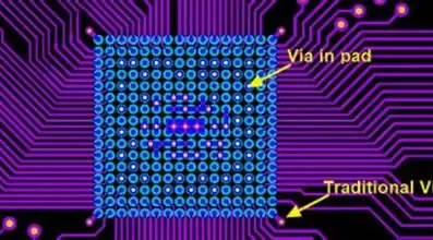
High-Density Interconnect (HDI) Implementation
High-density interconnect (HDI) technology employs microvias with diameters typically below 150 micrometers, often formed by laser drilling, together with fine line and space circuitry. Stacked or staggered microvia configurations allow connections across multiple layers while preserving board planarity. In robotic designs, HDI enables integration of high-pin-count processors, memory, and sensor interfaces on boards that fit within actuator housings. Sequential build-up processes add layers incrementally, supporting the complex routing needed for simultaneous motor control and real-time feedback loops. The approach also facilitates thinner overall constructions that reduce weight, an important factor for mobile and aerial robotic systems.
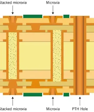
Best Practices for Reliable Robotic PCB Layouts
Begin with a thorough stackup review that places high-speed signals adjacent to reference planes and isolates noisy power domains. Route critical traces first, using blind and buried vias to maintain reference integrity and minimize layer transitions. Apply via-in-pad selectively under fine-pitch devices while verifying that the chosen via fill process meets thermal cycling requirements. Incorporate sufficient copper balancing and thermal relief patterns to limit warpage, especially in boards subjected to repeated temperature changes. Simulation of signal integrity, power integrity, and thermal performance before layout completion reduces the need for costly revisions. Documentation of layer-specific design rules ensures consistent manufacturing outcomes across production runs.
Reliability Considerations in Robotic Environments
Robotic PCBs experience continuous vibration, occasional shock, and wide temperature swings that can accelerate fatigue in interconnects. Proper via aspect ratios and fill materials mitigate cracking risks associated with thermal expansion mismatch. High-density interconnect (HDI) constructions require careful control of dielectric thickness and copper adhesion to maintain long-term insulation resistance. Multi-layer PCB design benefits from symmetric stackups that minimize bow and twist, preserving connector alignment and component solder joint integrity. Regular inspection criteria focus on via fill quality and surface planarity to support consistent assembly yields.
Conclusion
Advanced layout techniques centered on multi-layer PCB design, blind and buried vias, via-in-pad, and high-density interconnect (HDI) enable the compact, high-performance electronics essential to modern robotics. Structured application of these methods improves signal integrity, thermal management, and mechanical robustness while respecting manufacturing constraints. Engineers who integrate these practices early in the design cycle achieve reliable boards that meet the demanding operational profiles of robotic systems.
FAQs
Q1: How does multi-layer PCB design improve performance in robotic controllers?
A1: Multi-layer PCB design separates power, ground, and signal layers, reducing noise coupling and enabling controlled impedance routing for motor drivers and sensor interfaces. This separation supports higher component density and shorter interconnect lengths, which are critical in space-constrained robotic assemblies. The approach also enhances thermal spreading through dedicated inner copper planes.
Q2: What benefits do blind and buried vias provide compared with through vias in robotics PCBs?
A2: Blind and buried vias eliminate unnecessary via stubs, lowering parasitic effects that can impair high-speed signals in robotic communication links. They free surface area for component placement and allow routing on otherwise obstructed layers. The resulting higher interconnect density supports compact controller boards without compromising electrical performance.
Q3: When should via-in-pad be used in high-density robotic PCB layouts?
A3: Via-in-pad is appropriate when fine-pitch components such as processors or memory devices leave insufficient room for conventional fan-out routing. The technique shortens signal paths, improves thermal transfer, and maintains high routing density. Proper via fill and capping ensure reliable solder joints under the mechanical stresses typical of robotic operation.
Q4: How does high-density interconnect (HDI) support miniaturization in robotics?
A4: High-density interconnect (HDI) uses microvias and fine lines to achieve greater routing density within thinner board constructions. This enables integration of complex circuitry into smaller volumes suitable for actuators and end-effectors. The technology maintains signal integrity and mechanical stability required for reliable robotic function.
References
IPC-6012E — Qualification and Performance Specification for Rigid Printed Boards. IPC, 2017
IPC-A-600K — Acceptability of Printed Boards. IPC, 2020
JEDEC J-STD-020E — Moisture/Reflow Sensitivity Classification. JEDEC, 2014





