 ALLPCB


High-frequency RF systems demand precise control over signal paths, and a 12-layer PCB stackup provides the necessary flexibility to separate critical functions across multiple planes. Engineers working on wireless communication modules, radar systems, and high-speed data links frequently select this configuration to balance routing density with electromagnetic performance. The additional layers allow dedicated return paths and shielding structures that single- or double-sided boards cannot achieve. Proper arrangement of signal, ground, and power layers directly influences insertion loss, crosstalk, and overall system reliability in RF environments.
A 12-layer PCB RF stackup consists of alternating conductive copper layers and insulating dielectric materials arranged to support controlled impedance traces and effective isolation between circuits. This structure becomes particularly relevant when operating frequencies exceed several hundred megahertz, where even small deviations in trace geometry or dielectric properties can degrade performance. Industry professionals rely on such stackups to accommodate mixed-signal designs that combine sensitive RF front-ends with digital control circuitry on the same board. The configuration also supports higher component density without compromising the ground reference planes essential for return current paths. As RF applications continue to push toward millimeter-wave bands, the ability to maintain consistent electrical characteristics across the board becomes a primary design driver.
Why a 12-Layer PCB RF Stackup Matters
A 12-layer PCB RF stackup consists of alternating conductive copper layers and insulating dielectric materials arranged to support controlled impedance traces and effective isolation between circuits. This structure becomes particularly relevant when operating frequencies exceed several hundred megahertz, where even small deviations in trace geometry or dielectric properties can degrade performance. Industry professionals rely on such stackups to accommodate mixed-signal designs that combine sensitive RF front-ends with digital control circuitry on the same board. The configuration also supports higher component density without compromising the ground reference planes essential for return current paths. As RF applications continue to push toward millimeter-wave bands, the ability to maintain consistent electrical characteristics across the board becomes a primary design driver.
Technical Principles of Signal Performance in Multilayer RF Designs
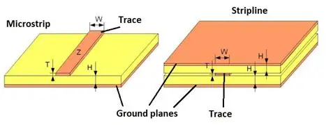
Signal propagation in RF circuits depends on maintaining consistent characteristic impedance along transmission lines, which a 12-layer PCB stackup achieves through careful selection of dielectric thickness and copper weight on specific layers. Ground planes placed adjacent to signal layers provide low-inductance return paths that reduce loop area and minimize radiated emissions. Dielectric materials with stable dissipation factors help limit signal attenuation, while the overall layer count permits stripline or microstrip configurations optimized for the target frequency range. Isolation between RF and digital sections improves when multiple ground planes are interleaved, creating Faraday-cage-like barriers that contain electromagnetic fields. Impedance matching across the 12-layer PCB RF stackup requires modeling of trace width, spacing, and reference plane proximity to achieve target values such as 50 ohms or 75 ohms.
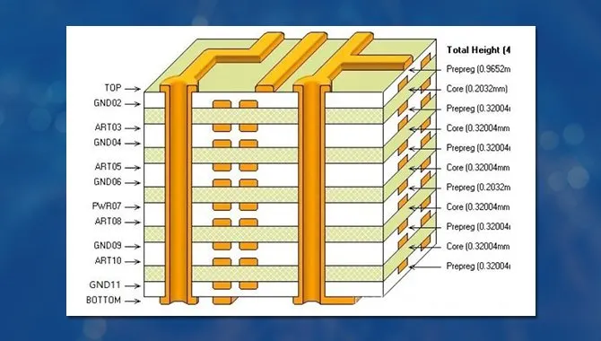
Signal loss mechanisms in high-frequency designs include conductor loss due to skin effect and dielectric loss arising from the loss tangent of the substrate. A 12-layer arrangement allows engineers to route critical RF traces on inner layers as striplines, where the signal is fully enclosed by ground planes, thereby reducing radiation and improving isolation. Power distribution networks benefit from dedicated planes that lower impedance at RF frequencies and provide stable voltage references. Thermal management also improves because additional copper layers can act as heat spreaders when connected appropriately. These principles align with established qualification practices outlined in IPC-6012E, which addresses performance requirements for rigid printed boards.
Best Practices for Designing a 12-Layer PCB RF Stackup
Designers begin by defining the required impedance targets and isolation levels before assigning functions to each layer in the 12-layer PCB stackup. Critical RF signals are typically placed on layers adjacent to continuous ground planes, while power planes occupy inner positions to minimize noise coupling. Dielectric materials are chosen based on their dielectric constant stability and loss characteristics across the operating temperature and frequency range. Trace geometry calculations account for manufacturing tolerances to ensure impedance remains within acceptable limits after fabrication. Ground stitching vias connect multiple reference planes, maintaining equipotential surfaces and reducing slot radiation.
Isolation between transmit and receive paths improves when sensitive signals are routed on separate layers separated by ground planes. Decoupling capacitor placement follows low-inductance paths to the nearest power and ground planes. Via transitions are minimized on RF routes, and when necessary, back-drilling or controlled-depth vias reduce stub effects that cause reflections. Thermal relief patterns on plane connections are sized to balance electrical performance with heat dissipation needs. These practices support consistent manufacturing outcomes referenced in IPC-A-600K for acceptability criteria of printed boards.
Practical Considerations for Material Selection and Layer Arrangement
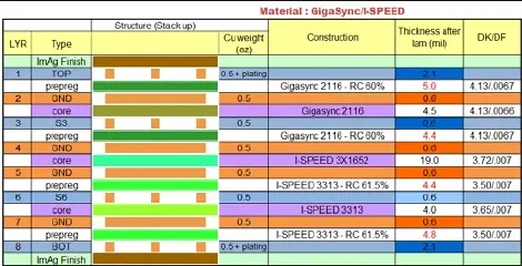
Material choice in a 12-layer PCB RF stackup centers on balancing electrical performance with mechanical stability and cost. Low-loss dielectrics reduce 12-layer PCB signal loss RF while maintaining dimensional stability during thermal cycling. Copper foil roughness affects conductor loss at higher frequencies, prompting selection of smoother foils for outer signal layers. Layer symmetry helps control warpage and ensures reliable registration during lamination. Prepreg and core thicknesses are selected to achieve the precise dielectric spacing needed for target impedances.
Conclusion
A carefully engineered 12-layer PCB RF stackup enables engineers to meet demanding signal integrity requirements in modern RF systems. Attention to impedance control, layer arrangement, and material properties directly reduces 12-layer PCB signal loss RF and enhances isolation. Following established qualification standards ensures the final assembly meets performance expectations across production volumes. These design choices ultimately support reliable operation in wireless, radar, and high-speed communication equipment.
FAQs
Q1: How does a 12-layer PCB RF stackup improve impedance matching compared with fewer layers?
A1: A 12-layer PCB RF stackup provides additional reference planes that allow precise control of trace geometry and dielectric spacing. This arrangement supports consistent characteristic impedance across longer routes and complex layouts. Engineers can dedicate specific layers to RF signals while maintaining solid ground returns, resulting in better matching and reduced reflections at target frequencies.
Q2: What factors contribute most to 12-layer PCB signal loss RF in high-frequency designs?
A2: Conductor losses from skin effect and dielectric losses from substrate dissipation factor are primary contributors. Proximity of signal traces to ground planes and the choice of low-loss materials help minimize attenuation. Proper via design and avoidance of unnecessary layer transitions further reduce loss mechanisms in the completed 12-layer PCB RF stackup.
Q3: How can designers achieve effective 12-layer PCB isolation RF between sensitive circuits?
A3: Multiple interleaved ground planes create shielding barriers that contain electromagnetic fields. Strategic placement of RF traces on inner stripline layers surrounded by grounds reduces crosstalk. Via fencing and careful partitioning of the board into isolated regions enhance overall isolation performance in the 12-layer PCB stackup.
Q4: Which materials are commonly evaluated for 12-layer PCB RF material selection?
A4: Engineers assess dielectric constant stability, loss tangent, and thermal expansion characteristics when choosing substrates. Materials with consistent properties across frequency and temperature ranges support reliable impedance control. The final selection balances electrical requirements with manufacturability and mechanical reliability for the intended 12-layer PCB RF stackup.
References
IPC-6012E — Qualification and Performance Specification for Rigid Printed Boards. IPC, 2017
IPC-A-600K — Acceptability of Printed Boards. IPC, 2020





