 ALLPCB


Introduction
Copper foil serves as the foundational conductive material in printed circuit boards, enabling the intricate pathways that power modern electronics. Electrical engineers encounter copper foil early in the PCB design process, where its thickness directly influences trace widths, current capacity, and signal integrity. Understanding the origins of this material reveals how raw copper transforms into the precise foils used in manufacturing. This journey spans mining, refining, and specialized production methods tailored for the electronic industry. By tracing copper foil back to its source, designers gain insights into selecting optimal thicknesses for reliable performance. The manufacturing process ensures consistency, aligning with standards that govern quality and performance.
What Is Copper Foil and Why It Matters in the PCB Design Process
Copper foil consists of a thin, continuous sheet of high-purity copper, typically laminated onto substrate materials like epoxy resin and glass fabric to form the core layers of a PCB. In the design process, engineers specify copper foil thickness to balance electrical performance, thermal management, and fabrication feasibility. Thinner foils support fine-pitch traces for high-density designs, while thicker ones handle higher currents in power sections. This selection impacts impedance control, where precise thickness ensures signal propagation matches simulations. During manufacturing, the foil undergoes etching to define circuit patterns, with its initial weight determining post-etch thickness. Adherence to IPC-2221 guidelines helps engineers calculate trace widths based on copper foil thickness, preventing overheating or voltage drops.
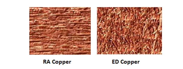
The relevance extends to high-frequency applications, where foil profile affects skin effect and insertion loss. Standard thicknesses range from 9 micrometers for high-speed signals to 70 micrometers for power delivery. Engineers must consider these properties during stackup development to avoid manufacturing defects like over-etching. Copper foil quality directly correlates with PCB reliability, making its source and production critical for consistent outcomes.
The Technical Principles Behind Copper Foil Production
Copper foil production begins with electrolytic copper cathodes derived from refined ore, achieving over 99.9 percent purity through smelting and electrolysis. The dominant method for PCB applications is electrodeposition, where copper ions in a sulfuric acid electrolyte deposit onto a rotating drum under direct current. As the drum spins, a uniform layer forms on its polished surface, which is then stripped, cleaned, and treated for adhesion. This process allows precise control over thickness by adjusting current density and drum speed, yielding foils from 5 to 140 micrometers. Electrodeposited foil features a shiny drum side and rougher matte side, optimized for lamination in manufacturing.
An alternative is the rolled annealed process, starting with cast copper ingots that undergo repeated hot and cold rolling followed by annealing to restore ductility. This method produces smoother, more flexible foil suited for flexible circuits but less common in rigid PCBs due to higher cost. Both techniques ensure the foil meets purity levels essential for low resistance and minimal impurities. Surface treatments, such as electrodeposition of zinc or chromium, enhance bonding to prepregs during lamination. These principles underpin the supply chain, transforming mined copper into engineering-grade material.
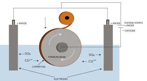
IPC-4562 classifies copper foils by type, profile, and grade, specifying electrodeposited versus rolled variants for different applications. Profiles range from standard to very low profile, influencing high-speed performance by reducing surface roughness.
Copper Foil Thickness Selection in the PCB Design Process
In the PCB design process, copper foil thickness dictates trace geometry and layer stackup configuration. Engineers use 1 ounce per square foot, equivalent to 35 micrometers, as a baseline for most signal layers, scaling up to 2 ounces for power planes. Thicker foils reduce the required trace width for a given current, per IPC-2221 current-carrying capacity charts, but increase etching difficulty and material cost. For multilayer boards, varying thicknesses across layers optimizes space and heat dissipation. Simulations verify that selected thicknesses maintain controlled impedance, crucial for RF and high-speed digital designs.
Manufacturing implications arise during panelization and imaging, where foil thickness affects registration accuracy. Thinner foils enable denser routing but demand tighter process controls to avoid warpage. Designers collaborate with fabricators early to confirm availability of specified weights, ensuring design rules align with production capabilities.
Manufacturing Considerations for Copper Foil Integration
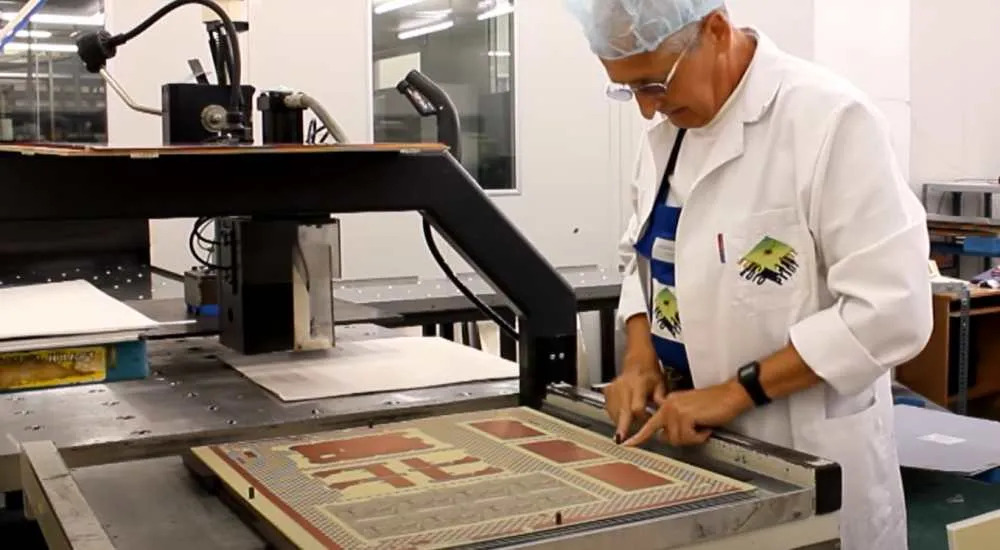
Once specified, copper foil integrates into PCBs via lamination, where it bonds to prepreg under heat and pressure in a vacuum press. The foil's surface treatment ensures mechanical and chemical adhesion, preventing delamination during thermal cycling. In multilayer manufacturing, inner layers form by imaging, etching excess copper, black oxide treatment, and alignment for subsequent lamination. Outer layers receive additional plating to build finished thickness, compensating for etching loss. IPC-6012 outlines qualification requirements, including minimum copper thickness post-fabrication to guarantee performance.
Quality checks verify foil uniformity using cross-section analysis and weight measurements. Variations in thickness can lead to inconsistent etch depths, affecting yield. For heavy copper designs, extended plating cycles deposit extra copper, demanding robust equipment and chemistry control. Engineers review these steps to refine designs for manufacturability.
Best Practices for Optimizing Copper Foil Thickness in Design and Manufacturing
Start with application needs: select thinner foils like 18 micrometers for high-density interconnects and thicker 70 micrometers for high-current paths. Reference IPC-2221 for trace width calculations, incorporating temperature rise limits. Balance cost by minimizing heavy copper layers, using it only where necessary. Incorporate design rule checks for minimum annular ring and spacing based on foil weight. During design reviews, simulate thermal profiles to validate dissipation.
In manufacturing handoff, provide detailed stackup drawings specifying foil weights and plating additions. Request tolerance data per IPC-6012 to ensure compliance. Test prototypes for actual thickness via microsectioning, adjusting future designs accordingly. These practices enhance reliability while streamlining production.
Conclusion
Copper foil originates from refined electrolytic copper, transformed via electrodeposition or rolling into the precise material vital for PCBs. Its thickness profoundly shapes the design process, influencing electrical, thermal, and mechanical performance. Manufacturing processes build on this foundation, adhering to standards like IPC-4562 and IPC-2221 for consistency. Electrical engineers benefit from understanding this supply chain, enabling informed selections that bridge design intent with fabrication reality. Prioritizing these elements yields robust, high-performance boards ready for electronic industry demands.
FAQs
Q1: What are the standard thicknesses for PCB copper foil in the design process?
A1: Standard PCB copper foil thicknesses include 18 micrometers (0.5 oz/ft2), 35 micrometers (1 oz/ft2), and 70 micrometers (2 oz/ft2), with finer options like 9 micrometers for high-density designs. Engineers select based on current requirements and signal speed during stackup planning. IPC-2221 provides charts for trace sizing, ensuring safe operation. Manufacturing tolerances maintain these values post-etching.
Q2: How does copper foil thickness impact PCB manufacturing?
A2: Copper foil thickness affects etching precision, plating needs, and lamination adhesion in manufacturing. Thicker foils require wider spaces to prevent shorts and longer etch times for undercutting control. Per IPC-6012, finished thicknesses must meet minimums for reliability. Designers specify weights to align with fab capabilities, reducing defects.
Q3: What is the primary manufacturing process for electronic industry copper foil?
A3: Electrodeposition dominates, depositing copper from electrolyte onto a rotating drum for uniform, high-purity foil used in rigid PCBs. This method controls thickness precisely for design process needs. Rolled annealed foil supplements for flex applications. IPC-4562 defines specifications for both, ensuring quality.
Q4: Why consider copper foil profile in high-speed PCB design?
A4: Foil profile influences skin effect and losses at high frequencies, with low-profile options per IPC-4562 minimizing roughness. Thinner effective skin depth demands smoother surfaces for signal integrity. Engineers balance this with adhesion during manufacturing reviews.
References
IPC-4562 — Metal Foil Specification for Printed Boards. IPC, 2013
IPC-2221B — Generic Standard on Printed Board Design. IPC, 2012
IPC-6012E — Qualification and Performance Specification for Rigid Printed Boards. IPC, 2015





