 ALLPCB


Copper weight in printed circuit boards directly influences electrical performance and thermal behavior. Standard 1 oz copper remains the default for most low to moderate power designs because it balances cost and manufacturability. In contrast, 3 oz copper provides substantially greater current carrying capacity and improved heat spreading. Engineers evaluate the choice based on application requirements rather than defaulting to thicker foil. The decision affects trace width calculations, layer stackup, and overall board reliability.
What Is Copper Weight and Why It Matters
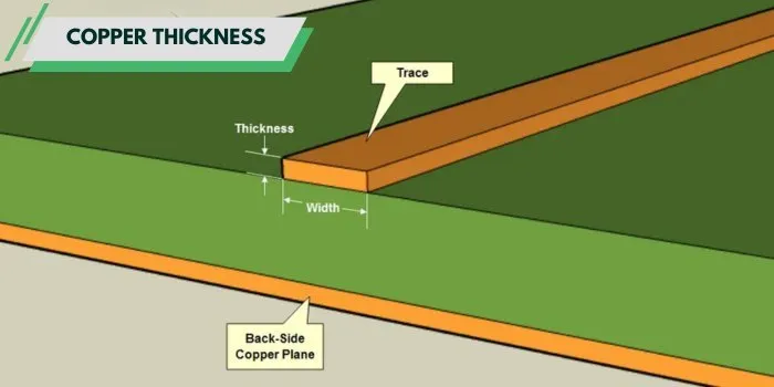
Copper weight expresses the mass of copper per square foot of board area. One ounce per square foot corresponds to a nominal thickness of 35 micrometers, while three ounces yields approximately 105 micrometers. This difference scales the cross sectional area available for current flow and heat conduction. Higher copper weight becomes relevant when designs must handle elevated currents without excessive temperature rise or voltage drop. Procurement and design teams review copper weight early because it influences material selection and fabrication processes. Industry specifications such as IPC 6012E define qualification requirements for rigid boards that incorporate varying copper thicknesses.
Technical Principles of Copper Thickness in PCBs
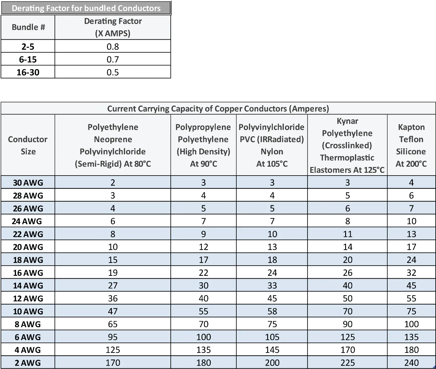
Current carrying capacity increases with copper cross section according to established thermal models. A trace in 3 oz copper can support roughly three times the current of an equivalent width trace in 1 oz copper before reaching the same temperature rise. Heat dissipation improves because the thicker foil acts as a larger thermal mass and conduction path. Etching finer features becomes more challenging with thicker copper because undercut and trace definition tolerances widen. Warpage risk can increase during thermal cycling if copper distribution is unbalanced across layers. IPC A 600K provides acceptance criteria for finished boards that help verify trace integrity and copper thickness uniformity after fabrication.
PCB Performance Comparison: 3 oz versus 1 oz Copper
Electrical resistance drops proportionally with increased copper thickness for the same trace geometry. This reduction lowers I squared R losses in power distribution networks. Thermal resistance from component to ambient also decreases, allowing higher power dissipation in the same footprint. However, the minimum achievable trace width and spacing typically increase with 3 oz copper due to etching limitations. Impedance control for high speed signals requires careful modeling because the thicker conductor alters the effective dielectric spacing and fringing fields. Cost rises because more copper material is consumed and processing steps such as plating and etching require additional time or chemistry adjustments.
PCB Application Suitability and Cost Benefit Analysis
High current power supplies, motor drivers, and LED lighting arrays often benefit from 3 oz copper when space constraints prevent widening traces sufficiently in 1 oz material. Automotive and industrial controls that experience wide temperature swings may select thicker copper to maintain performance margins. Consumer electronics and low power digital boards rarely justify the added expense because 1 oz copper meets all requirements with simpler fabrication. Cost benefit analysis weighs the price premium of heavier copper against savings in board area or the elimination of additional cooling hardware. Material properties such as peel strength and thermal expansion must remain compatible with the chosen laminate system throughout the operating temperature range.
Practical Guidance for Selecting Copper Weight
Begin by calculating the required trace width for target current and allowable temperature rise using industry accepted methods. Compare the resulting dimensions against available board space and routing density. If 1 oz traces become impractically wide, evaluate 3 oz copper or consider additional copper layers. Review the full stackup for copper balance to minimize warpage during reflow and operation. Consult fabrication notes early to confirm achievable minimum features and plating capabilities for the selected copper weight. JEDEC J STD 020E addresses moisture sensitivity considerations that remain relevant regardless of copper thickness but can interact with thicker foil during assembly thermal profiles.
Conclusion
Selecting 3 oz copper over standard 1 oz material delivers clear advantages in current capacity and thermal performance when application demands exceed the limits of thinner foil. The choice requires systematic evaluation of electrical, thermal, and manufacturing constraints. Proper adherence to qualification and acceptance standards ensures the final board meets performance and reliability targets. Engineers who integrate copper weight decisions into the earliest design phases achieve more compact and cost effective solutions.
FAQs
Q1: When should designers consider 3 oz copper versus 1 oz copper PCB?
A1: Designers evaluate 3 oz copper when calculated trace widths in 1 oz material exceed available routing space or when thermal analysis shows unacceptable temperature rise under expected load currents. The thicker foil provides greater cross sectional area for both current flow and heat spreading while maintaining acceptable voltage drop. Cost and manufacturability trade offs are assessed against the specific application requirements.
Q2: How does copper weight affect PCB performance comparison metrics?
A2: Copper weight directly scales current carrying capacity and thermal conductivity along the conductor plane. Three ounce copper reduces resistive losses and improves heat dissipation compared with one ounce copper for identical trace geometries. Trace impedance and etching tolerances also change, requiring updated modeling for signal integrity and manufacturability.
Q3: What factors enter a PCB cost benefit analysis for heavier copper?
A3: Material cost, processing time, and achievable feature sizes contribute to the overall expense of 3 oz copper boards. Savings may appear in reduced board area, fewer layers, or elimination of external heatsinks. Long term reliability under high current or thermal cycling conditions further influences the economic justification.
Q4: Which industry standards guide copper thickness selection in PCBs?
A4: IPC 6012E outlines qualification and performance requirements for rigid printed boards that incorporate different copper weights. Complementary documents such as IPC A 600K define visual and dimensional acceptance criteria that apply after fabrication regardless of chosen copper thickness.


