ALLPCB


If you're working on a printed circuit board (PCB) design and considering via-in-pad technology, you might be wondering about the potential challenges and how to dodge them. Via-in-pad design, where a via is placed directly on a component pad, can save space and improve signal integrity, but it comes with risks like soldering issues, thermal problems, and manufacturing hiccups. In this blog, we'll dive deep into the common pitfalls of via-in-pad design—focusing on PCB design mistakes, via-in-pad errors, soldering issues, thermal problems, and manufacturing problems—and provide practical solutions to help you achieve a reliable and efficient design.
What Is Via-in-Pad Design and Why Use It?
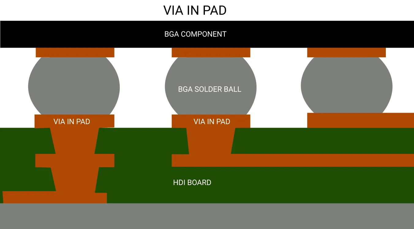
Via-in-pad design is a technique in PCB layout where a via—a small hole that connects different layers of the board—is placed directly within the pad of a surface-mounted component. This approach is often used in high-density designs, especially for components like ball grid arrays (BGAs) with fine pitch (spacing less than 0.8 mm). By placing vias on pads, designers can save valuable board space, shorten trace lengths, and enhance signal integrity by reducing parasitic inductance, which can be as high as 1-2 nH per via in traditional designs.
However, while the benefits are clear, via-in-pad design introduces unique challenges that can lead to costly errors if not addressed. Let’s explore the most common pitfalls and how to avoid them in your next project.
Common Pitfalls in Via-in-Pad Design
1. Soldering Issues: Solder Wicking and Voiding
One of the most frequent via-in-pad errors is related to soldering. When a via is placed on a pad, solder paste can flow into the via during reflow soldering, a phenomenon known as solder wicking. This can result in insufficient solder on the pad, leading to weak or incomplete joints. Additionally, air or flux trapped in the via can cause voiding—empty spaces in the solder joint—that compromises connection reliability. Studies suggest that voiding rates above 25% can significantly reduce the mechanical strength of solder joints.
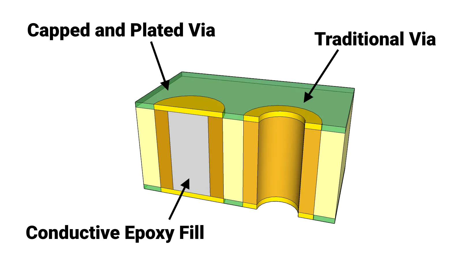
Solution: To prevent solder wicking, consider filling the via with a non-conductive epoxy or using a via plugging process before soldering. This blocks the via and stops solder from flowing in. Another approach is to use smaller via sizes (e.g., 0.2 mm or less) to minimize the amount of solder that can escape. Additionally, optimize your stencil design by reducing the aperture size over via-in-pad areas to control solder paste volume.
2. Thermal Problems: Uneven Heat Distribution
Thermal issues are another major concern in via-in-pad designs. Vias conduct heat away from the pad during soldering, which can lead to uneven heat distribution. This often results in cold solder joints, where the solder doesn’t fully melt or bond with the component. For high-power components dissipating heat above 1 W, this can also cause long-term reliability issues, as the via may act as a heat sink, pulling heat away from where it’s needed.
Solution: To manage thermal problems, incorporate thermal relief patterns around the via-in-pad area. These patterns limit the heat dissipation through the via by connecting the pad to the ground plane with thin traces, typically 0.2-0.3 mm wide. Additionally, ensure your PCB design software accounts for thermal mass during simulation to predict and address potential hot or cold spots. If possible, avoid placing vias on pads for high-power components unless absolutely necessary for space constraints.
3. Manufacturing Problems: Fabrication and Assembly Challenges
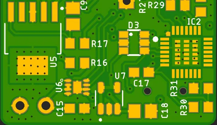
Manufacturing problems often arise with via-in-pad designs due to the complexity they add to the fabrication and assembly process. For instance, unfilled vias can trap contaminants or moisture during the manufacturing process, leading to corrosion or electrical shorts over time. Moreover, during assembly, misalignment of components over via-in-pad structures can cause poor contact or even open circuits, especially with fine-pitch components where tolerances are as tight as 0.1 mm.
Solution: Work closely with your PCB manufacturer to ensure they can handle via-in-pad designs. Specify whether the vias should be filled or plugged, and confirm the materials and processes they use. Use design for manufacturability (DFM) guidelines to set appropriate via sizes and pad dimensions—typically, vias should be at least 0.15 mm smaller in diameter than the pad to avoid alignment issues. Finally, provide clear documentation in your design files to indicate via-in-pad locations and any special requirements.
4. Signal Integrity Issues: Parasitic Effects and Crosstalk
While via-in-pad designs can reduce trace length and improve signal integrity, they can also introduce parasitic capacitance and inductance if not designed carefully. For high-speed signals above 1 GHz, these parasitic effects can cause signal degradation or crosstalk between adjacent vias. A poorly placed via-in-pad might increase return path inductance by 0.5-1 nH, enough to affect signal timing in sensitive applications like DDR memory interfaces.
Solution: Use simulation tools to model the impact of via-in-pad structures on signal integrity before finalizing your layout. Keep via lengths as short as possible by using thinner PCB stack-ups where feasible. For high-speed designs, consider back-drilling or using blind vias to minimize stub lengths, which can reduce parasitic effects. Additionally, space via-in-pad structures at least 0.5 mm apart from other high-speed signal vias to lower the risk of crosstalk.
5. Mechanical Stress and Reliability Concerns
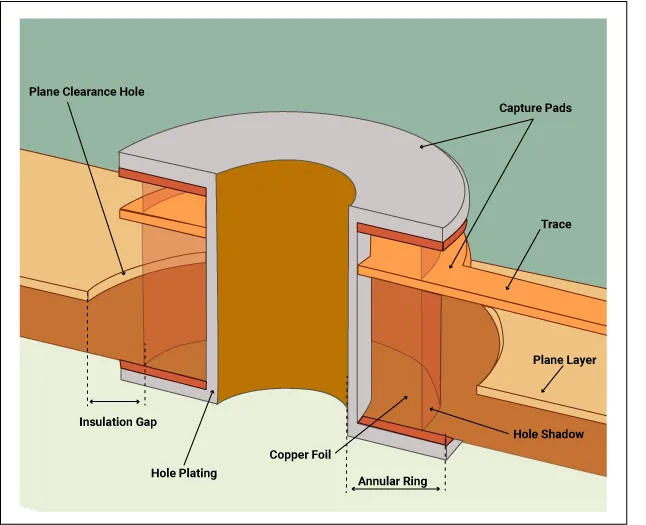
Placing a via directly on a pad can create mechanical stress points on the PCB, especially under thermal cycling or vibration. The difference in thermal expansion between the via barrel (often copper with a coefficient of 17 ppm/°C) and the surrounding laminate (around 14-16 ppm/°C) can lead to cracks or delamination over time. This is a critical concern for automotive or aerospace applications where boards may experience temperature swings from -40°C to 85°C.
Solution: Reinforce via-in-pad areas by ensuring proper copper plating thickness, typically 25-30 μm, to withstand mechanical stress. Avoid placing via-in-pad structures near board edges or areas prone to flexing. If reliability is a top concern, consider alternative routing strategies to move vias off pads, even if it means slightly increasing board size. Additionally, conduct thermal cycling tests during prototyping to validate the design under real-world conditions.
Best Practices for Successful Via-in-Pad Design
Now that we've covered the common pitfalls—soldering issues, thermal problems, manufacturing problems, and more—let’s summarize some best practices to ensure your via-in-pad design is robust and reliable.
- Collaborate Early with Manufacturers: Engage with your PCB fabricator and assembler during the design phase to understand their capabilities and limitations for via-in-pad structures.
- Use Appropriate Via Sizes: Stick to microvias (diameters of 0.1-0.2 mm) for via-in-pad designs to minimize solder wicking and thermal dissipation issues.
- Incorporate Via Filling: Opt for conductive or non-conductive via filling to prevent solder escape and improve structural integrity, especially for vias under 0.3 mm in diameter.
- Leverage Simulation Tools: Use PCB design software with built-in thermal and signal integrity simulation to catch potential issues before manufacturing.
- Follow IPC Standards: Adhere to industry standards like IPC-4761 for via protection and filling to ensure consistent quality and reliability.
Conclusion: Mastering Via-in-Pad Design for Better PCBs
Via-in-pad design offers significant advantages for high-density PCB layouts, but it’s not without its challenges. By understanding and addressing common PCB design mistakes like soldering issues, thermal problems, and manufacturing problems, you can avoid costly via-in-pad errors and create boards that perform reliably in demanding applications. Whether you're working on a compact consumer device or a high-speed industrial system, the solutions and best practices outlined here—such as via filling, thermal reliefs, and early manufacturer collaboration—can help you achieve a successful design.
Take the time to plan your layout carefully, simulate potential issues, and follow industry guidelines. With these steps, you’ll be well-equipped to tackle the complexities of via-in-pad design and deliver PCBs that meet both performance and reliability goals.