ALLPCB


If you're looking to ensure your printed circuit board (PCB) design is ready for production without costly delays or defects, manufacturability checks are your key to success. By following a PCB manufacturability checklist, adhering to design for manufacturability guidelines, and conducting a thorough DFM analysis, you can avoid common PCB manufacturing defects and streamline the production process. In this comprehensive guide, we'll take a deep dive into the importance of manufacturability checks, offering actionable insights and practical tips to help you achieve flawless PCB production.
What Are PCB Manufacturability Checks and Why Do They Matter?
Manufacturability checks are a critical step in the PCB design process. They involve evaluating your design against a set of rules and guidelines to ensure it can be fabricated and assembled without issues. Known as Design for Manufacturability (DFM), this process helps identify potential problems early, saving time, reducing costs, and improving the overall quality of the final product.
Without proper manufacturability checks, even a well-designed PCB can encounter issues like misaligned components, insufficient clearances, or material incompatibilities during production. These problems can lead to delays, increased costs, or even complete redesigns. By integrating a PCB design rules check and DFM analysis into your workflow, you can catch these issues before they become expensive mistakes.
Understanding Design for Manufacturability (DFM) Guidelines
Design for Manufacturability (DFM) is a set of best practices that optimize a PCB design for efficient production. These guidelines focus on aligning your design with the capabilities and limitations of manufacturing equipment and processes. Let's explore some core DFM principles that form the foundation of a solid PCB manufacturability checklist.
1. Component Placement and Spacing
Proper placement of components is essential to avoid assembly issues. Components placed too close together can cause soldering problems, such as bridging, where solder unintentionally connects adjacent pads. A general rule of thumb is to maintain a minimum spacing of 0.2 mm between surface-mount components to allow for accurate placement and soldering.
Additionally, ensure that taller components, like electrolytic capacitors, are placed away from shorter ones to avoid shadowing during the soldering process. Shadowing can prevent smaller components from receiving adequate heat, leading to poor solder joints.
2. Trace Width and Clearance
Trace width and clearance are critical for ensuring signal integrity and preventing short circuits. For standard designs, a minimum trace width of 0.15 mm (6 mils) and a clearance of 0.15 mm between traces are often recommended for most fabrication processes. However, for high-current applications, trace widths may need to be wider—sometimes up to 0.5 mm or more—depending on the current load. You can calculate the required width using online trace width calculators based on current, copper thickness (typically 1 oz/ft2 or 35 μm), and temperature rise.
Failure to adhere to these guidelines can result in PCB manufacturing defects like trace breakage or unintended electrical connections. Always check your design against the fabrication house's specific capabilities to avoid issues.
3. Via Design and Placement
Vias connect different layers of a PCB, but improper design can lead to manufacturing challenges. For example, vias smaller than 0.3 mm in diameter may be difficult to drill accurately, increasing the risk of defects. Additionally, placing vias too close to pads (less than 0.25 mm) can cause solder wicking, where solder flows into the via instead of bonding the component.
To avoid these issues, follow DFM guidelines by using standard via sizes and ensuring sufficient spacing from pads and traces. If you're working on a high-density design, consider using microvias, but confirm that your manufacturer supports this technology.
Building a Comprehensive PCB Manufacturability Checklist
A well-structured PCB manufacturability checklist acts as a roadmap to ensure your design is production-ready. Below, we've outlined key areas to focus on during your DFM analysis to minimize risks and enhance manufacturability.
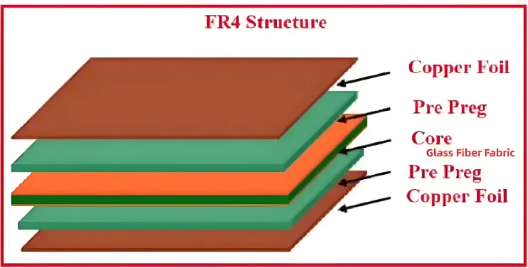
1. Material Selection
Choosing the right materials is a foundational step in PCB design. Standard FR-4 material is suitable for most applications due to its cost-effectiveness and reliability. However, for high-frequency designs, you might need materials like Rogers or Teflon, which offer lower dielectric constants (typically around 2.2 to 3.5 compared to FR-4's 4.5) to reduce signal loss.
Ensure that your chosen material is compatible with the manufacturer's processes and meets your design requirements for thermal and electrical performance. Mismatched materials can lead to delamination or poor performance during operation.
2. Layer Stack-Up Design
The layer stack-up defines how different layers of your PCB are arranged, impacting signal integrity and manufacturability. For a 4-layer board, a common stack-up might include a top signal layer, a ground plane, a power plane, and a bottom signal layer. This arrangement helps reduce electromagnetic interference (EMI) and ensures stable power distribution.
During DFM analysis, verify that the stack-up aligns with the manufacturer's capabilities, especially for impedance-controlled designs. For instance, achieving a 50-ohm impedance for high-speed signals often requires specific layer thicknesses and dielectric constants, which should be calculated and confirmed early in the design phase.
3. Solder Mask and Silkscreen
Solder mask protects the PCB from oxidation and prevents solder bridges during assembly. Ensure that the solder mask clearance around pads is at least 0.1 mm to avoid overlap, which can interfere with soldering. Similarly, silkscreen text or markings should be legible, with a minimum line width of 0.15 mm and placed away from pads and vias to prevent confusion during assembly.
Neglecting these details can lead to PCB manufacturing defects, such as incomplete soldering or misaligned components due to unclear markings.
4. Panelization and Fiducials
Panelization involves arranging multiple PCBs on a single panel for efficient manufacturing. Ensure that breakaway tabs or V-scoring lines are placed correctly to allow easy separation without damaging the boards. Additionally, include fiducial markers—small copper dots used for machine alignment during assembly—at least three per board, placed near the corners for optimal accuracy.
Skipping fiducials or poor panelization can result in misalignment during assembly, leading to costly rework.
Common PCB Manufacturing Defects and How to Avoid Them
Even with a robust design, manufacturing defects can occur if DFM guidelines are not followed. Here are some common issues and tips to prevent them through a thorough PCB design rules check.
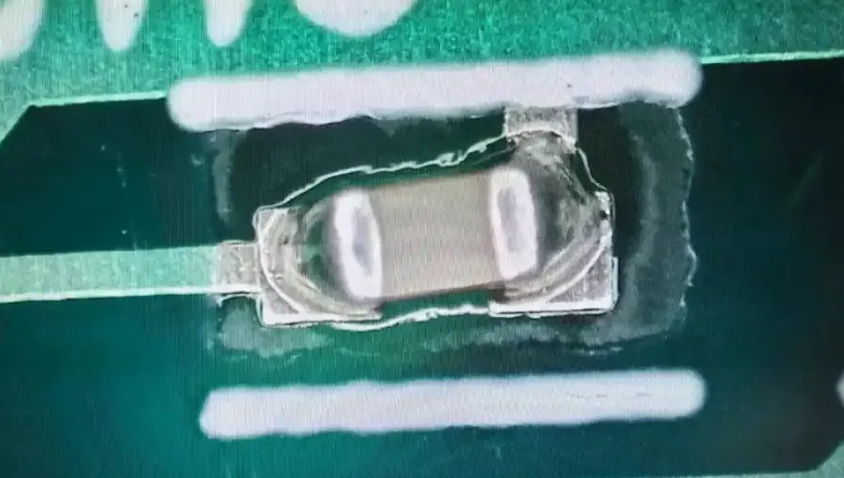
1. Tombstoning
Tombstoning occurs when a small surface-mount component, like a resistor, stands on one end due to uneven soldering. This often happens when pads are too large or when there's a thermal imbalance during reflow soldering. To prevent this, ensure pad sizes match the component footprint (typically within 0.1 mm tolerance) and balance the thermal mass around the component by adding copper fills if needed.
2. Solder Bridges
Solder bridges form when excess solder connects adjacent pads, creating a short circuit. This is often caused by insufficient spacing between pads or poor solder mask design. Maintain a minimum pad-to-pad spacing of 0.2 mm and verify that the solder mask fully covers areas between pads to minimize this risk.
3. Incomplete Etching
Incomplete etching leaves unwanted copper on the PCB, potentially causing short circuits. This defect often results from overly thin traces or insufficient spacing during design. Stick to minimum trace widths and clearances recommended by your manufacturer, and perform a thorough DFM analysis to catch these issues before production.
Conducting a PCB Design Rules Check (DRC)
A PCB design rules check (DRC) is an automated process within most design software that validates your layout against a set of predefined rules. These rules cover aspects like trace spacing, via sizes, and component clearances. Running a DRC is a critical part of DFM analysis, as it helps identify potential manufacturability issues before sending the design for fabrication.
For example, if your design includes a trace clearance of 0.1 mm but the manufacturer's minimum is 0.15 mm, the DRC will flag this as an error. Addressing these errors early ensures that your design aligns with production capabilities, reducing the likelihood of delays or defects.
Most design tools allow you to customize DRC rules based on your manufacturer's specifications. Take the time to input accurate values for parameters like minimum drill size (e.g., 0.3 mm) and annular ring width (e.g., 0.15 mm) to ensure a thorough check.
Collaborating with Your Manufacturer for Optimal Results
One of the most effective ways to ensure manufacturability is to collaborate closely with your fabrication and assembly partner. Share your design files early for a preliminary DFM review, and request feedback on potential issues. Many manufacturers provide specific design guidelines, such as minimum trace widths or supported stack-up configurations, which can be integrated into your PCB manufacturability checklist.
Additionally, consider requesting a prototype run before full-scale production. Prototyping allows you to test the design in real-world conditions and identify any unforeseen issues, such as signal integrity problems in high-speed circuits (e.g., signal delays exceeding 100 ps due to improper impedance matching).
Conclusion: Mastering PCB Manufacturability for Success
Unlocking PCB success starts with a commitment to manufacturability checks. By following design for manufacturability guidelines, building a detailed PCB manufacturability checklist, and conducting a thorough DFM analysis, you can avoid common PCB manufacturing defects and ensure a smooth production process. Incorporating a PCB design rules check into your workflow further minimizes risks, helping you deliver high-quality boards on time and within budget.
Whether you're designing a simple 2-layer board or a complex multilayer system, the principles of manufacturability remain the same. Pay attention to component spacing, trace design, material selection, and manufacturer collaboration to achieve optimal results. With these strategies in hand, you're well on your way to creating reliable, production-ready PCBs that meet your project goals.