 ALLPCB


Solder mask serves as a critical protective layer in printed circuit board fabrication. It insulates conductive traces, prevents solder bridges during assembly, and shields the board from environmental factors. Material pricing for solder mask directly influences overall PCB fabrication cost analysis, particularly for designs destined for high-volume production or demanding applications. Engineers and procurement teams must evaluate these costs alongside performance requirements to maintain project budgets without compromising reliability. Standard processes and material selections often provide the most predictable pricing structures in the supply chain.
What Is Solder Mask and Why Material Costs Matter
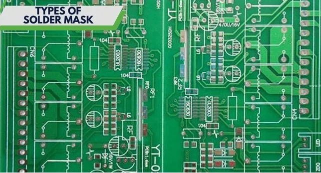
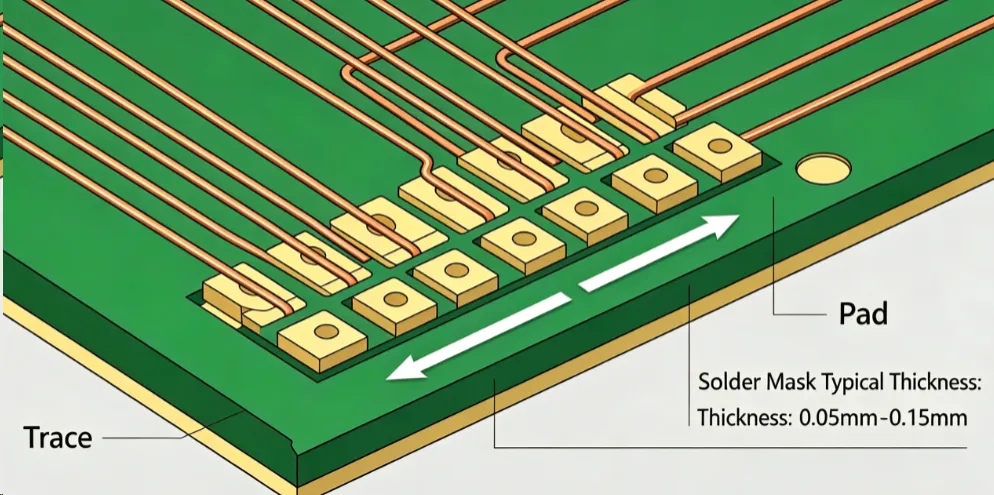
Solder mask, also known as solder resist, consists of a polymer-based coating applied to the outer layers of a PCB. It covers copper traces while exposing pads and vias for component attachment. The choice of material type, such as liquid photoimageable formulations or dry film alternatives, determines both functional properties and associated expenses in fabrication. In PCB fabrication cost analysis, solder mask can represent a noticeable portion of material and processing overhead, especially when specialized properties are required. Understanding these elements helps teams balance electrical performance, manufacturability, and total project expenditure.
Industry standards guide material qualification and performance expectations. IPC-SM-840 outlines qualification and performance requirements for permanent solder mask, including classes that differentiate between telecommunications and high-reliability applications. Compliance with such specifications ensures consistent quality but can influence material selection and pricing.
Technical Factors Influencing Solder Mask Material Pricing
Several engineering variables affect solder mask material pricing during PCB production. The base polymer chemistry, whether epoxy-based or modified for enhanced thermal or chemical resistance, contributes to raw material expenses. Application methods, including screen printing, spray coating, or curtain coating, require different equipment setups and process controls that factor into overall costs. Board size, layer count, and trace density further influence the volume of material consumed and the precision needed during patterning.
Color selection represents another practical consideration. Standard green formulations typically align with the most common production workflows, while other hues may necessitate additional pigment adjustments or separate material batches. Thickness specifications also play a role, as they must meet dielectric and coverage requirements without excess application that increases usage. Environmental classifications, such as halogen-free compositions, add formulation complexity that can elevate pricing relative to conventional options.
Design features like fine-pitch areas or dense via fields demand higher-resolution materials and tighter process tolerances. These elements tie directly into PCB fabrication cost analysis because they affect yield rates and rework potential. Volume commitments allow fabricators to optimize material procurement and reduce per-unit expenses through economies of scale.
Engineering Mechanisms Behind Cost Variations
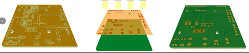
The mechanisms driving cost differences stem from material formulation and process integration. Liquid photoimageable solder mask cures via ultraviolet exposure after precise patterning, enabling fine feature definition but requiring controlled viscosity and photosensitivity. Dry film alternatives laminate as a solid sheet, offering uniform thickness yet potentially higher material waste on irregular board surfaces. Both approaches must satisfy adhesion, hardness, and insulation criteria defined in relevant standards.
Process parameters such as curing temperature profiles and development chemistry influence throughput and defect rates. Higher-reliability classes under IPC-SM-840 impose stricter testing for thermal shock, humidity resistance, and dielectric strength, which often correlate with premium material grades. These requirements translate into elevated pricing because they demand validated formulations and additional quality verification steps during fabrication.
Board complexity amplifies these effects. Multilayer designs with controlled impedance or high-frequency characteristics may pair solder mask selection with specific laminate properties, creating interdependencies that affect total material budgeting. Procurement teams analyzing PCB fabrication costs therefore review stack-up details alongside solder mask specifications to identify optimization opportunities.
Practical Strategies for Cost-Effective Solder Mask Selection
Design for manufacturability practices provide the most direct path to reducing solder mask costs. Specifying standard green liquid photoimageable material with conventional thickness ranges aligns with established production lines and minimizes setup variations. Early collaboration between design and fabrication teams helps identify opportunities to simplify pad and trace layouts that reduce the precision demands on the mask layer.
Volume planning supports more favorable material pricing through consolidated orders. Engineers can evaluate whether a single standard formulation meets all functional needs across multiple projects rather than specifying custom variants for each board. Process audits during quoting stages often reveal whether alternative application methods deliver equivalent performance at lower overall expense.
Adherence to IPC-6012E guidelines for rigid printed boards ensures that solder mask performance integrates properly with the complete board qualification process. This alignment avoids over-specification that unnecessarily increases material grades. Regular review of design rules for minimum dam widths and clearance tolerances further supports efficient material usage without compromising assembly yields.
Conclusion
Solder mask material pricing arises from a combination of formulation chemistry, application processes, color and thickness choices, and compliance with performance standards. Systematic evaluation of these factors within PCB fabrication cost analysis enables engineers to identify targeted adjustments that maintain quality while controlling expenses. Standard selections and design optimizations consistently deliver the most reliable outcomes across diverse production scenarios. Teams that incorporate these considerations early in the design cycle achieve more predictable budgeting and smoother transitions to manufacturing.
FAQs
Q1: How does solder mask color affect material pricing in PCB projects?
A1: Standard green solder mask aligns with common production workflows and typically supports lower costs compared to alternative colors. Non-standard colors require additional pigment handling or separate material sourcing, which can increase expenses in PCB fabrication cost analysis. Selecting green where performance allows helps maintain cost effectiveness without affecting electrical or assembly requirements.
Q2: What role does IPC-SM-840 play in solder mask material selection?
A2: IPC-SM-840 defines qualification and performance criteria for permanent solder mask, including separate classes for different end-use environments. Engineers reference these classes when specifying materials to ensure the chosen formulation meets reliability needs. This standard-based approach supports consistent quality while guiding decisions that influence overall material pricing.
Q3: How can design choices help reduce solder mask costs during fabrication?
A3: Optimizing trace spacing, via placement, and feature density reduces the demands on material resolution and coverage uniformity. Early application of design for manufacturability principles allows fabricators to use standard processes and formulations. These adjustments contribute directly to lowering expenses identified in PCB fabrication cost analysis.
Q4: What factors should procurement teams review when evaluating cost-effective solder mask options?
A4: Teams examine material type, required performance class, board volume, and any special environmental properties against standard offerings. Comparing these elements against baseline green liquid photoimageable options reveals opportunities for savings. Integration with broader PCB fabrication cost analysis ensures selections balance technical needs and budget constraints.
References
IPC-SM-840 — Qualification and Performance of Permanent Solder Mask. IPC
IPC-6012E — Qualification and Performance Specification for Rigid Printed Boards. IPC, 2017
IPC-A-600K — Acceptability of Printed Boards. IPC, 2020





