 ALLPCB


Robotics systems depend on control printed circuit boards to manage motors, sensors, and communication interfaces with precision. These boards operate in demanding environments that expose them to vibration, temperature fluctuations, and continuous duty cycles. Engineers frequently encounter faults that disrupt motion control or data exchange between subsystems. Effective robotics PCB troubleshooting begins with systematic fault finding rather than random component replacement. This approach minimizes downtime and preserves the integrity of the overall robotic platform.
Control PCBs in robotics integrate power distribution networks, microcontroller units, and signal conditioning circuits. Failures often originate from power rail instability, electromagnetic interference, or mechanical stress on solder joints. Understanding these mechanisms allows technicians to isolate problems before they propagate through the system. Industry standards such as IPC-A-610 provide acceptance criteria for assembly quality that help prevent many latent defects during initial build.
Common Causes of Failures in Robotics Control PCBs
Power supply irregularities rank among the most frequent issues. Voltage drops or excessive ripple on rails that feed motor drivers can cause erratic behavior in servo loops. Thermal cycling accelerates oxidation at contact points and induces micro-cracks in traces or vias. Signal integrity problems arise when high-speed communication lines experience crosstalk or impedance mismatches, leading to corrupted encoder feedback or command packets.
Component degradation also contributes significantly. Electrolytic capacitors lose capacitance over time under elevated temperatures, while MOSFETs in power stages suffer from threshold voltage shifts after repeated switching events. Manufacturing-related defects, including insufficient solder volume or misaligned components, create intermittent connections that manifest only under load. Following J-STD-001 guidelines for soldering processes reduces the incidence of such assembly-related faults.
Mechanical factors play a distinct role in robotic applications. Vibration from actuators can fatigue leads and solder fillets, particularly on boards mounted near moving joints. Contamination from dust or lubricants may create conductive paths that trigger spurious signals. Systematic PCB fault finding therefore requires consideration of both electrical and environmental contributors.
Diagnostic Techniques for Effective Fault Finding
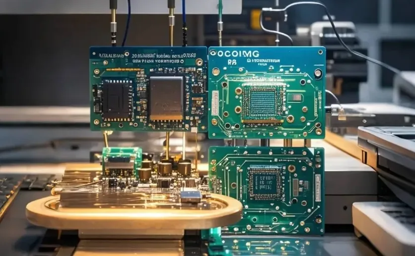
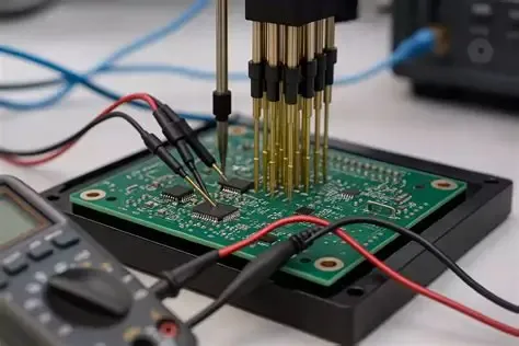
Begin troubleshooting with visual inspection under adequate lighting and magnification. Look for discoloration, lifted pads, or foreign material bridging conductors. Next, perform voltage measurements at key test points referenced to the board ground plane. Compare readings against expected values derived from the schematic while the system operates under controlled conditions.
Signal tracing follows voltage checks when digital or analog communication appears compromised. An oscilloscope connected to critical nets reveals waveform distortion, ringing, or missing transitions. Probe placement should avoid introducing additional capacitance that alters high-frequency behavior. Component testing with a multimeter or dedicated analyzer verifies passive devices and semiconductor junctions without removing parts initially.
Thermal imaging provides non-contact insight into localized overheating that indicates excessive current draw or poor thermal transfer. Compare images taken during idle and loaded states to pinpoint anomalies. These methods together form a layered approach that narrows the fault location efficiently.
Rework and Repair Procedures
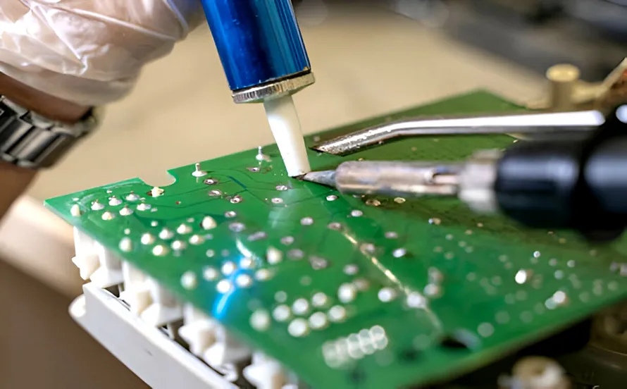
Once the faulty section is isolated, rework begins with proper preparation. Desoldering tools must be temperature-controlled to avoid damaging adjacent components or the substrate. Replacement parts should match original specifications for voltage rating, tolerance, and package type. After installation, inspect the joint quality to ensure adequate fillet formation and absence of bridges.
Signal integrity restoration may require adding decoupling capacitors or rerouting traces on prototype boards. For production units, follow documented repair procedures that maintain original layout characteristics. Post-repair functional testing under simulated robotic loads confirms that the fix restores normal operation without introducing new issues.
Documentation of each step, including measurements before and after, supports future diagnostics on similar platforms. Consistent application of these practices improves overall repair success rates and reduces repeat failures.
Best Practices for Sustained Reliability
Preventive measures reduce the need for corrective action. Regular inspection intervals aligned with operational hours help detect early signs of wear. Environmental controls such as conformal coating application protect against moisture and contaminants in industrial settings. Design reviews that incorporate adequate trace widths and thermal relief patterns further enhance robustness.
Training maintenance teams on standardized fault-finding sequences ensures repeatable results across different robotic installations. Maintaining spare boards with pre-verified configurations allows rapid swap-out when on-site repair time is limited. These strategies collectively support higher uptime in automated systems.
Conclusion
Systematic robotics PCB troubleshooting combines electrical measurements, signal tracing, and component testing to resolve issues efficiently. Adherence to established assembly and soldering standards minimizes preventable defects from the outset. Practical rework techniques, when executed with care, restore functionality while preserving board integrity. Engineers who apply these methods consistently achieve more reliable robotic control systems and reduced maintenance overhead.
FAQs
Q1: How does signal tracing support robotics PCB troubleshooting?
A1: Signal tracing uses an oscilloscope to monitor waveforms along critical paths, revealing distortions or interruptions that voltage measurements alone cannot detect. This technique helps isolate communication or control signal faults in motor driver or sensor circuits.
Q2: What role do voltage measurements play in PCB fault finding?
A2: Voltage measurements at designated test points identify power rail deviations, ground shifts, or regulator failures that affect overall board operation. Accurate readings under load conditions guide subsequent component testing and repair decisions.
Q3: When is component testing required during repair of robotics control PCBs?
A3: Component testing becomes necessary after initial voltage and signal checks fail to locate the issue, allowing verification of individual parts such as capacitors, transistors, or integrated circuits without full board disassembly.
Q4: What considerations apply to rework on densely populated robotics PCBs?
A4: Rework requires temperature-controlled tools, precise part matching, and post-repair inspection to avoid collateral damage to nearby components or traces while restoring original electrical performance.
References
IPC-A-610G — Acceptability of Electronic Assemblies. IPC, 2017
J-STD-001H — Requirements for Soldered Electrical and Electronic Assemblies. IPC, 2020
IPC-6012E — Qualification and Performance Specification for Rigid Printed Boards. IPC, 2017





