 ALLPCB


Introduction
In the realm of advanced PCB design, moving beyond basic footprints requires a deep understanding of how land patterns interact with modern components and manufacturing processes. As electronic devices shrink and performance demands rise, engineers face challenges with complex footprints for fine-pitch components and high-density interconnect structures. These elements are crucial for achieving reliable solder joints, minimizing defects, and ensuring signal integrity in compact assemblies. This article explores sophisticated techniques that electrical engineers can apply to optimize footprints, drawing on established principles to enhance yield and longevity. By mastering these methods, designers can tackle the intricacies of high-density interconnect boards while adhering to proven engineering practices.
Understanding Complex Footprints in Advanced PCB Design
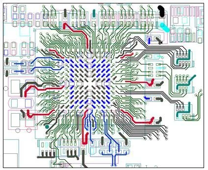
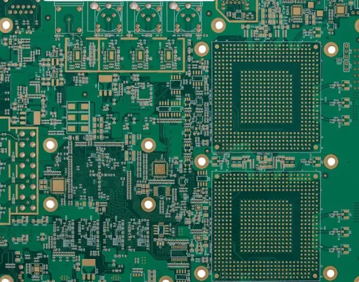
Complex footprints deviate from standard through-hole or coarse-pitch surface-mount patterns, incorporating features like exposed pads, microvia integration, and precise geometries for components such as BGAs and QFNs. In advanced PCB design, these footprints must accommodate tolerances in component placement, solder paste volume, and reflow profiles to prevent issues like bridging or voids. The relevance stems from the push toward miniaturization, where high-density interconnect demands footprints that support denser routing without compromising thermal or electrical performance. Engineers must consider not just pad size but also courtyard definitions and fiducial marks to facilitate automated assembly. Failure to address these complexities can lead to higher rework rates and field failures, underscoring the need for systematic design approaches.
Key Technical Principles for Fine-Pitch Components
Fine-pitch components, often with lead spacings below 0.5 mm, require land patterns that balance solder joint formation with inspectability and reworkability. The IPC-7351B standard outlines three density levels—Most Likely, Nominal, and Least—to guide pad dimensions based on fabrication and assembly capabilities. For instance, the Most Likely level provides smaller pads suited to high-volume production, optimizing space for high-density interconnect while maintaining joint integrity. Heel, toe, and side fillet dimensions are calculated to ensure proper solder flow during reflow, accounting for component lead deformation and paste release. Electrical engineers should evaluate these parameters using component datasheets alongside standard guidelines to avoid over-etching or insufficient overlap.
Another principle involves solder mask defined versus non-solder mask defined pads, where the former uses mask openings smaller than copper for finer control in fine-pitch arrays. This technique reduces bridging risks but demands precise mask registration. Thermal relief patterns in via-in-pad structures dissipate heat evenly, preventing solder wicking that could starve joints. These mechanisms ensure mechanical strength and electrical connectivity under thermal cycling.
Designing Footprints for High-Density Interconnect (HDI)
High-density interconnect PCBs integrate microvias, blind vias, and buried vias directly into footprints to escape fine-pitch components efficiently. In advanced PCB design, stacked or staggered microvias within BGA pads allow direct routing to inner layers, minimizing trace lengths and inductance. Engineers must specify via fill types, such as conductive epoxy, to maintain planarity and support subsequent lamination cycles. Complex footprints here incorporate dog-bone escapes or via clusters, with anti-pads sized to prevent shorts during plating. The J-STD-001 standard provides criteria for acceptable via-in-pad solder joints, emphasizing fillet height and void limits.
Layer stackup influences footprint viability, as thinner dielectrics enable tighter via aspect ratios around 0.8:1 for laser-drilled microvias. Fiducials scaled to local feature density aid alignment in multi-step HDI buildup processes. By aligning footprint design with HDI capabilities, engineers achieve routing densities exceeding traditional methods.
Best Practices for Advanced Footprint Implementation
Start with component datasheet analysis to extract body dimensions, lead pitch, and terminal geometry, then apply IPC-7351B density levels appropriate for the assembly process. For fine-pitch components, select the Most Likely level to maximize board real estate, verifying pad-to-pad spacing exceeds minimum routing widths. Incorporate courtyard boundaries at least 0.25 mm beyond the component outline to prevent interference, and add test points or probes where signal integrity demands it. Solder paste release simulations guide stencil thickness, typically 75-100 microns for fine-pitch, ensuring 50-75% paste coverage on pads.
Thermal management in complex footprints involves spoke-style reliefs on exposed pads, with spoke widths tuned to current carrying needs. For QFN devices, central thermal pads require multiple vias tented with solder mask to control voiding. Perform design rule checks for annular ring integrity and mask expansion, usually 50-75 microns, to accommodate registration tolerances. Validate designs through thermal modeling and DFM reviews before fabrication.
Iterate with cross-functional input from fabrication and assembly teams to refine tolerances. Document footprint libraries with revision controls, including 3D models for step-and-repeat verification.
Case Study: Optimizing a Fine-Pitch BGA Footprint
Consider a scenario involving a 0.4 mm pitch BGA with 400+ balls in a high-density interconnect application. Initial designs using Nominal density pads resulted in frequent bridging during reflow due to excessive paste volume. Switching to Most Likely dimensions per IPC-7351B, combined with 0.1 mm microvias in peripheral pads, reduced escape layer needs by 30%. Staggered via placement avoided resonance issues, while filled vias ensured flatness for lid attachment.
Post-assembly analysis revealed improved joint shear strength, aligning with J-STD-001 criteria. This adjustment not only boosted yield from 85% to 98% but also shortened signal paths, enhancing high-speed performance. The case highlights how targeted footprint tweaks resolve real-world constraints in advanced PCB design.
Conclusion
Advanced PCB footprint design elevates from rote application to strategic engineering, enabling reliable integration of fine-pitch components and high-density interconnect features. By leveraging standards like IPC-7351B and principled approaches to pad geometry, thermal relief, and via integration, engineers mitigate risks and unlock performance potential. Practical implementation demands iterative validation and process awareness, ensuring designs translate seamlessly to production. Mastering these techniques positions teams to innovate in compact, high-reliability electronics.
FAQs
Q1: What are the main density levels in IPC-7351B for complex footprints?
A1: IPC-7351B defines Most Likely, Nominal, and Least density levels for land patterns in advanced PCB design. Most Likely suits high-density interconnect with compact pads for optimal space use. Nominal balances reworkability and density, while Least prioritizes inspectability. Select based on assembly capabilities to ensure reliable solder joints for fine-pitch components.
Q2: How do microvias impact footprint design for fine-pitch components?
A2: Microvias enable direct fanout from fine-pitch pads in high-density interconnect, reducing trace lengths and inductance. Place them within pad peripheries using staggered or stacked configurations for multi-layer escapes. Ensure via fill and tenting to maintain coplanarity. This technique supports pitches below 0.5 mm while adhering to fabrication limits.
Q3: Why is thermal relief critical in advanced PCB footprints?
A3: Thermal relief patterns in via-in-pad footprints prevent solder wicking and ensure even heat distribution during reflow. Spoke or radial designs balance thermal conductance with joint integrity for complex footprints. They are essential for fine-pitch components carrying high currents in high-density interconnect boards. Proper sizing avoids voids and enhances reliability.
Q4: What best practices improve yield for HDI footprints?
A4: Align complex footprints with HDI stackups, using IPC-7351B for pad sizing and precise mask expansion. Incorporate fiducials and courtyards for alignment. Simulate paste release and perform DFM checks to minimize bridging in fine-pitch areas. Cross-team reviews refine designs for production success.


