 ALLPCB


Introduction
High-power electronic systems generate significant heat during operation, and effective thermal management is essential to maintain performance and reliability. Four-ounce copper PCBs provide increased conductor thickness that supports higher current carrying capacity and improved heat spreading compared with standard one-ounce constructions. This capability proves particularly valuable in applications such as high-power LED lighting, power converters, and motor drives where localized heat concentrations can degrade components or shorten service life. Engineers therefore evaluate copper weight early in the design cycle to balance electrical requirements with thermal performance. Proper thermal management in 4 oz copper PCB designs reduces the risk of hotspots and supports stable operation under continuous load.
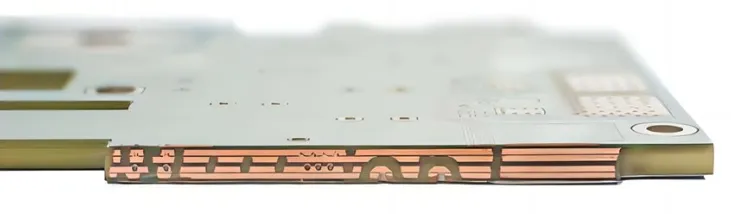
Understanding 4 oz Copper PCBs and Heat Dissipation Needs
Four-ounce copper refers to a copper foil weight of four ounces per square foot, resulting in approximately 140 micrometers of conductor thickness. This heavier copper lowers electrical resistance and increases the cross-sectional area available for heat conduction along traces and planes. In high-power LED PCB assemblies, the combination of forward current and optical conversion losses creates substantial thermal loads that must be removed efficiently. Without adequate heat dissipation paths, junction temperatures rise, reducing luminous output and accelerating lumen depreciation. The thicker copper layer acts as a built-in heat spreader, complementing external cooling solutions such as heatsinks or thermal interface materials. Designers therefore specify 4 oz copper when current densities exceed the limits of thinner foils while still requiring compact board layouts.
Thermal Management Principles in Thick Copper Designs
Heat transfer in PCBs occurs primarily through conduction along copper traces and planes, with secondary contributions from convection and radiation at board surfaces. Increasing copper thickness reduces thermal resistance in the plane of the board, allowing heat to spread more uniformly before reaching the edges or mounting points. Thermal vias filled or plated with copper further enhance vertical heat flow to inner layers or to the opposite side of the board. Material selection for the dielectric also influences overall thermal performance, as the resin and glass weave exhibit lower thermal conductivity than copper. Industry guidelines such as those in IPC-6012E address the qualification requirements for rigid boards that must withstand thermal cycling without delamination or excessive warpage. Effective thermal design therefore integrates copper geometry, via placement, and stackup choices to create low-resistance heat paths.
Design Strategies for Effective PCB Heat Dissipation
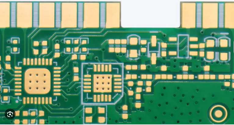
Layout practices begin with identifying high-dissipation components and allocating sufficient copper area around them. Wide traces or solid copper pours connected to these components increase the effective heat-spreading surface. Thermal relief patterns around pads are minimized or eliminated in high-current paths to maintain low thermal resistance. Arrays of thermal vias placed directly beneath component thermal pads conduct heat to internal or bottom-side copper planes. Board orientation and enclosure airflow are considered to promote natural or forced convection. When additional cooling is required, mechanical attachment points for heatsinks are incorporated during the mechanical design phase. These strategies are applied iteratively through simulation and prototype testing to verify that junction temperatures remain within component specifications.
Manufacturing and Quality Considerations
During fabrication, consistent copper plating thickness and via fill quality directly affect thermal performance. Controlled impedance and etch compensation become more critical with heavier copper because trace width tolerances influence both electrical and thermal characteristics. Inspection criteria defined in IPC-A-600K help ensure that finished boards meet acceptability standards for copper distribution, via fill, and surface finish integrity. Warpage control is especially important in thick-copper boards because differential expansion between copper and dielectric can induce stress during thermal cycling. Manufacturers therefore monitor lamination parameters and apply appropriate press cycles to maintain flatness. These process controls support the long-term reliability of 4 oz copper PCB thermal management solutions in demanding environments.
Applications in High Power LED PCB Systems
High-power LED arrays used in industrial lighting, automotive headlights, and horticultural systems benefit directly from 4 oz copper constructions. The thick copper planes distribute heat away from LED junctions toward board edges or dedicated thermal pads that interface with heatsinks. Proper trace routing also minimizes voltage drop along power distribution paths, reducing additional self-heating. When multiple LEDs operate in close proximity, thermal coupling between devices must be managed through copper pour segmentation or strategic via placement. System-level thermal resistance calculations include the LED package, solder joint, PCB copper, and external cooling path to predict steady-state temperatures. This integrated approach ensures that luminous efficacy and color stability remain consistent over the operating life of the luminaire.
Conclusion
Four-ounce copper PCBs offer a practical means to enhance heat dissipation in high-current and high-power applications without requiring excessively large board areas. By combining increased conductor thickness with thoughtful via placement, copper geometry, and adherence to established qualification standards, engineers achieve reliable thermal performance. Manufacturing processes that maintain plating uniformity and dimensional stability further support these design goals. When applied systematically, these principles enable compact, efficient electronic assemblies that meet both electrical and thermal requirements across a range of operating conditions.
FAQs
Q1: What factors influence 4 oz copper PCB thermal management performance?
A1: Copper thickness, trace width, via density, dielectric material properties, and external cooling methods all contribute to overall heat dissipation capability. Designers evaluate current density and component power dissipation early to determine the required copper weight and layout features. Following established qualification practices helps ensure the finished board maintains structural integrity under thermal stress. Simulation combined with prototype measurements validates that junction temperatures stay within acceptable limits for the target application.
Q2: How does 4 oz copper improve PCB heat dissipation compared with standard weights?
A2: The greater cross-sectional area of four-ounce copper reduces both electrical resistance and in-plane thermal resistance, allowing heat to spread more effectively from localized sources. This built-in spreading complements thermal vias and external heatsinks, lowering peak temperatures in high-power LED PCB designs. The approach is especially useful when board real estate is limited and high current must be carried without excessive temperature rise.
Q3: What layout techniques support effective thermal management on 4 oz copper boards?
A3: Solid copper pours connected to heat-generating components, dense thermal via arrays under component pads, and minimized thermal reliefs on power traces all lower thermal resistance. Component placement that aligns high-dissipation devices with board mounting points or airflow paths further aids heat removal. These techniques are refined through iterative design reviews to balance electrical, mechanical, and thermal objectives.
Q4: Are there industry standards relevant to 4 oz copper PCB quality and thermal reliability?
A4: Qualification and acceptability criteria for rigid printed boards address copper thickness consistency, via integrity, and resistance to thermal cycling. Adherence to these standards supports long-term reliability when boards operate under elevated temperatures. Manufacturers apply process controls that maintain flatness and plating quality, which are essential for consistent thermal performance in finished assemblies.
References
IPC-6012E - Qualification and Performance Specification for Rigid Printed Boards. IPC, 2017
IPC-A-600K - Acceptability of Printed Boards. IPC, 2020





