 ALLPCB


Backdrilling removes conductive stubs from plated through holes in printed circuit boards. This process improves signal integrity in high speed designs by minimizing reflections and crosstalk. Engineers select substrates carefully because material properties directly affect drilling precision, thermal behavior, and long term reliability. The choice between standard and specialized laminates influences both manufacturing yield and electrical performance. Proper material selection supports consistent results across production volumes.
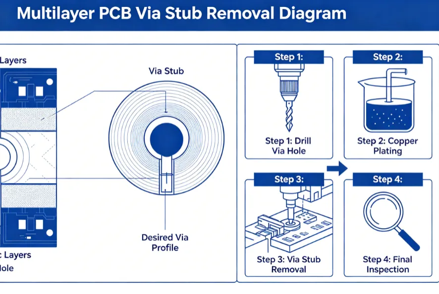
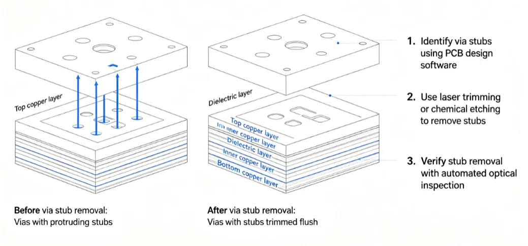
Backdrilling targets the unused portion of a via barrel after component attachment. Controlled depth drilling from the opposite side removes the stub without damaging functional layers. This technique proves essential in high frequency circuits where even small discontinuities degrade performance. Material selection for backdrilling determines how cleanly the drill bit cuts through copper and dielectric without causing excessive heat or mechanical stress. Substrates with stable mechanical properties reduce the risk of layer separation during the operation.
High frequency PCB substrates often replace conventional options when operating frequencies exceed several gigahertz. These materials exhibit lower dielectric constants and reduced loss tangents compared with standard FR4 backdrilling candidates. The reduced signal attenuation supports longer trace lengths and higher data rates. Engineers evaluate thermal expansion coefficients to ensure the substrate withstands the localized heating that occurs during backdrilling. Consistent material behavior across temperature cycles maintains via integrity after the process completes.
Understanding Backdrilling and Its Relevance to PCB Performance
Backdrilling targets the unused portion of a via barrel after component attachment. Controlled depth drilling from the opposite side removes the stub without damaging functional layers. This technique proves essential in high frequency circuits where even small discontinuities degrade performance. Material selection for backdrilling determines how cleanly the drill bit cuts through copper and dielectric without causing excessive heat or mechanical stress. Substrates with stable mechanical properties reduce the risk of layer separation during the operation.
High frequency PCB substrates often replace conventional options when operating frequencies exceed several gigahertz. These materials exhibit lower dielectric constants and reduced loss tangents compared with standard FR4 backdrilling candidates. The reduced signal attenuation supports longer trace lengths and higher data rates. Engineers evaluate thermal expansion coefficients to ensure the substrate withstands the localized heating that occurs during backdrilling. Consistent material behavior across temperature cycles maintains via integrity after the process completes.
Key Material Properties Influencing Backdrilling Success
Dielectric constant and dissipation factor rank among the primary electrical parameters. Lower values in these properties support better high frequency transmission after backdrilling. Mechanical strength and glass transition temperature affect how the laminate responds to the drilling forces and subsequent thermal excursions. Moisture absorption rates also matter because absorbed water can vaporize during drilling and create voids or delamination.
Coefficient of thermal expansion in the z axis requires particular attention. Mismatch between copper and dielectric expansion can induce stress around the via after backdrilling. Materials engineered for improved thermal stability maintain registration accuracy through multiple lamination and drilling cycles. Surface finish compatibility further influences drill bit life and hole wall quality. These interrelated properties guide the decision between standard epoxy glass systems and advanced resin formulations.
Material Selection Strategies for Different Application Requirements
Standard FR4 remains suitable for many moderate speed designs where backdrilling addresses moderate stub lengths. Its widespread availability and established processing parameters simplify qualification. When signal frequencies increase or trace lengths extend, low loss PCB materials become preferable. These substrates reduce insertion loss and allow tighter control over impedance after stub removal.
Selection begins with a review of required operating frequency, data rate, and environmental conditions. Engineers compare loss tangent values across candidate materials while also assessing drillability and post drill cleanliness. Thermal reliability testing confirms that the chosen substrate withstands reflow profiles without degradation around the backdrilled features. Cost considerations balance performance gains against manufacturing complexity. Documentation of these trade-offs supports consistent decisions across design teams.
Practical Guidelines for Implementing Backdrilling with Selected Substrates
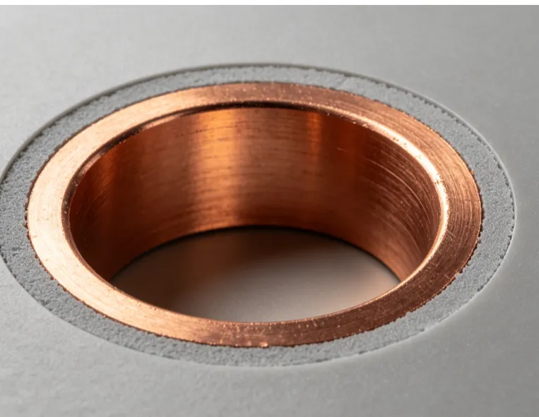
Process parameters must align with the chosen laminate. Feed rate, spindle speed, and peck depth settings vary according to resin system and glass weave style. Pilot runs verify hole wall quality and confirm that backdrilling depth remains within tolerance. Inspection after drilling checks for resin smear, glass fiber protrusion, and copper burrs that could affect subsequent plating or assembly.
Design rules incorporate backdrilling allowances from the start. Via placement avoids dense areas where heat buildup might compromise material integrity. Layer stack up planning ensures sufficient dielectric thickness above and below the target depth. Collaboration between design and manufacturing teams identifies potential issues early. Qualification follows established industry practices to verify both electrical and mechanical outcomes.
Conclusion
Effective backdrilling depends on matching substrate characteristics to the electrical and mechanical demands of the application. Standard FR4 backdrilling works well for many designs, while high frequency PCB substrates deliver superior performance when loss and signal integrity become critical. Systematic evaluation of dielectric properties, thermal behavior, and process compatibility leads to reliable results. Consistent application of these principles supports high yield production and long term product reliability.
FAQs
Q1: What factors determine the best substrate for backdrilling PCB materials?
A1: Material selection considers dielectric constant, loss tangent, thermal expansion, and moisture absorption. These properties influence drilling quality and signal performance after stub removal. Engineers also review glass transition temperature and drillability to ensure manufacturing compatibility.
Q2: How does FR4 backdrilling compare with low loss PCB materials at high frequencies?
A2: FR4 provides adequate performance for many moderate speed applications. Low loss materials reduce signal attenuation and reflections when frequencies rise. The choice depends on required data rates and acceptable insertion loss budgets.
Q3: Why is material selection for backdrilling important for high frequency PCB substrates?
A3: Appropriate substrates maintain impedance control and minimize discontinuities after via modification. They also resist thermal and mechanical stress during drilling. Proper selection improves overall yield and long term reliability.
Q4: What industry standards guide backdrilling and substrate evaluation?
A4: Qualification follows IPC-6012E for rigid printed board performance. Acceptability criteria appear in IPC-A-600K. These documents establish baseline requirements for material and process verification. IPC-2221B provides generic design guidance applicable to via planning and stack-up considerations.
References
IPC-6012E - Qualification and Performance Specification for Rigid Printed Boards. IPC, 2017
IPC-A-600K - Acceptability of Printed Boards. IPC, 2020
IPC-2221B - Generic Standard on Printed Board Design. IPC, 2012


