 ALLPCB


The Material Matters: Selecting Substrates for Optimal Performance in Minimum Size PCBs
Miniaturization continues to drive innovation across electronics, pushing designers toward smaller printed circuit boards that still deliver reliable electrical, thermal, and mechanical performance. Substrate choice directly influences whether a compact board meets its functional requirements or encounters issues such as excessive warpage, signal loss, or thermal runaway. Engineers must therefore evaluate material properties with the same rigor applied to circuit layout and component placement. This article examines the key considerations for PCB substrate selection in minimum size applications and provides structured guidance based on established engineering principles.
Why Substrate Selection Matters for Small PCBs
A PCB substrate serves as the foundational dielectric layer that supports conductive traces, provides electrical insulation, and manages heat and mechanical stresses. In boards with reduced footprints, the same material volume must handle higher current densities, tighter trace spacing, and increased component packing. Poor material selection can lead to dimensional instability during fabrication or assembly, compromising yield and long-term reliability. Industry standards such as IPC-6012E establish qualification requirements that help ensure substrates perform consistently even when board dimensions shrink. Consequently, understanding how properties like coefficient of thermal expansion, glass transition temperature, and dielectric constant interact with size constraints becomes essential for successful design.
Technical Principles Governing Substrate Behavior
Several interrelated material properties determine suitability for minimum size PCBs. Coefficient of thermal expansion mismatch between the substrate and copper or attached components generates stresses during temperature cycling; in small boards these stresses concentrate over shorter distances and can cause delamination or via cracking. Dielectric constant and loss tangent affect signal propagation speed and attenuation, which become critical when high-speed traces occupy limited real estate. Thermal conductivity governs heat spreading from concentrated power sources, while moisture absorption influences dimensional stability and electrical performance after reflow. Mechanical strength, quantified through metrics such as flexural modulus, must resist handling and vibration loads that are proportionally more severe on reduced board areas. These properties do not act in isolation; trade-offs frequently arise, for example between low dielectric constant for signal integrity and higher thermal conductivity for heat dissipation.
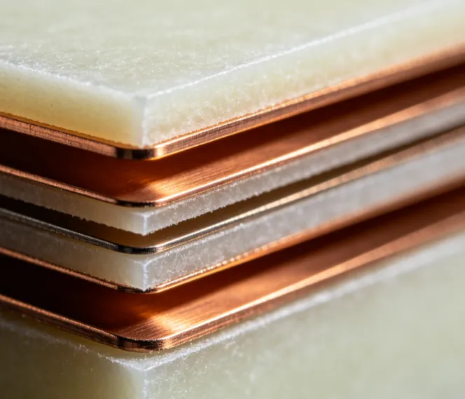
Warpage represents another critical mechanism in small PCBs. During lamination, reflow, or thermal cycling, uneven expansion or contraction across the stack-up produces out-of-plane deformation. Standards such as IPC-A-600K define acceptable warpage limits that become harder to meet as board size decreases because the same absolute deviation represents a larger percentage of the overall dimension. Material selection influences warpage through resin content, reinforcement type, and cure shrinkage characteristics. Designers therefore model stack-up symmetry and select substrates with matched in-plane expansion coefficients to keep warpage within specification.
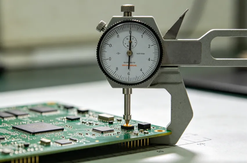
Practical Approaches to Material Selection
Effective PCB material selection begins with a clear definition of operating environment, signal requirements, and assembly processes. Engineers compile a requirements matrix that lists maximum operating temperature, frequency range, power dissipation, and expected thermal cycles. This matrix guides comparison of candidate substrates against property data sheets, focusing on values verified through standardized test methods. For high-frequency small PCBs, materials with stable dielectric properties across temperature and humidity ranges receive priority. When thermal management dominates, substrates offering higher thermal conductivity or metal-core constructions are evaluated, provided they satisfy electrical insulation needs.
Stack-up planning complements material choice. Symmetric constructions and balanced copper distribution reduce the risk of warpage in compact boards. Via aspect ratios must remain within fabricator capabilities, which often tightens as board thickness decreases to maintain mechanical integrity. Compliance with relevant standards, including those addressing moisture sensitivity during reflow, helps prevent defects that become more probable in densely populated small assemblies. Iterative simulation of thermal and mechanical behavior, followed by prototype builds, validates selections before volume production.
Conclusion
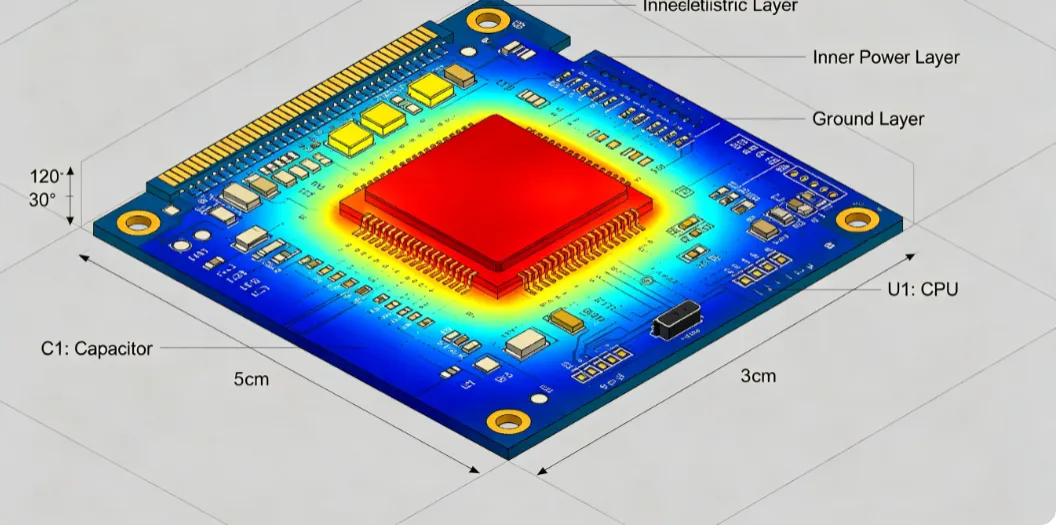
Substrate selection for minimum size PCBs requires systematic attention to thermal, electrical, and mechanical properties within the constraints imposed by reduced dimensions. By aligning material characteristics with application demands and adhering to established qualification standards, engineers achieve reliable performance without compromising board miniaturization goals. Thorough requirements definition, property evaluation, and stack-up optimization form the foundation of successful outcomes.
FAQs
Q1: What factors determine the best PCB substrate for minimum size applications?
A1: Key factors include coefficient of thermal expansion, dielectric properties, thermal conductivity, and moisture absorption. These properties must be balanced against the specific electrical, thermal, and mechanical demands of the compact design while satisfying qualification requirements outlined in standards such as IPC-6012E.
Q2: How do PCB material properties affect performance in small PCBs?
A2: Material properties influence signal integrity through dielectric constant and loss, thermal management through conductivity, and mechanical reliability through expansion behavior and strength. In reduced board sizes, mismatches or deficiencies in these properties produce amplified effects on warpage, via integrity, and long-term reliability.
Q3: Why is PCB material selection critical for high-performance small PCBs?
A3: High-performance small PCBs often operate at elevated frequencies or power levels within tight spaces. Appropriate substrate selection ensures adequate heat spreading, controlled impedance, and dimensional stability, thereby meeting performance targets without increasing overall board footprint.
Q4: What role do industry standards play in selecting substrates for compact PCBs?
A4: Standards such as IPC-A-600K and JEDEC J-STD-020E provide acceptance criteria and test methods that verify substrate performance under fabrication, assembly, and operating conditions. Reference to these standards helps ensure consistent quality and reliability across miniaturized designs.
References
IPC-6012E — Qualification and Performance Specification for Rigid Printed Boards. IPC, 2017
IPC-A-600K — Acceptability of Printed Boards. IPC, 2020
JEDEC J-STD-020E — Moisture/Reflow Sensitivity Classification. JEDEC, 2014





