 ALLPCB


Stacked vias enable high-density interconnects in multilayer printed circuit boards by aligning conductive paths through successive layers. When thermal conditions vary during assembly or operation, these structures experience mechanical stresses that can compromise long-term performance. Effective thermal management addresses heat flow and expansion differences to maintain via integrity. Engineers must consider these factors early in the design process to support reliable operation in demanding applications.
Why Stacked Via Thermal Management Matters
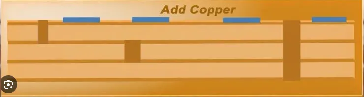
Stacked vias consist of multiple plated through-holes or microvias placed directly atop one another to conserve board space and shorten signal paths. This configuration increases routing density but also concentrates thermal loads in localized areas. Heat generated by active components travels through the board, and inadequate dissipation raises temperatures around the via stack. The resulting thermal gradients contribute to reliability concerns that affect product lifespan and field performance.
Industry standards such as IPC-6012E establish qualification requirements for rigid printed boards, including aspects relevant to via construction and thermal endurance. Proper attention to stacked via thermal management therefore supports compliance and reduces the risk of premature failures in assembled boards.
Technical Principles of Thermal Stress in Stacked Vias
Coefficient of thermal expansion mismatch between copper conductors and surrounding dielectric materials creates internal stresses during temperature changes. Copper expands and contracts at a different rate than typical epoxy-glass laminates, producing shear and tensile forces at the via walls and interfaces. Repeated thermal cycling amplifies these effects through fatigue mechanisms that can initiate cracks or delamination.
Heat dissipation paths in stacked via regions depend on copper thickness, via diameter, and proximity to thermal relief features. When heat cannot escape efficiently, localized hot spots develop and accelerate stress accumulation. Thermal vias placed near stacked vias help distribute heat more evenly across the board, lowering peak temperatures and reducing the magnitude of expansion differentials.
Warpage of the printed board during thermal excursions further complicates via reliability. Uneven heating or cooling causes the substrate to bend, imposing additional bending moments on the via stack. These mechanical loads combine with CTE-induced stresses and can exceed the fracture toughness of the plating or the adhesion between layers.
Best Practices for Thermal Management Around Stacked Vias
Designers improve heat dissipation by incorporating dedicated thermal vias adjacent to signal or power stacked vias. These thermal vias increase the effective copper cross-section for conduction and connect to larger copper planes that act as heat spreaders. Placement rules typically maintain a minimum distance to avoid interfering with signal integrity while still providing thermal relief.
Material selection influences overall thermal performance. Laminates with lower CTE values in the z-axis reduce expansion mismatch with copper and limit stress during reflow and operational temperature swings. Controlled copper plating thickness in the vias also contributes to mechanical robustness under thermal load.
Manufacturing processes must maintain consistent via filling and plating quality to avoid voids that act as stress concentrators. Standards such as IPC-A-600K define acceptability criteria for printed board features, including via wall quality and surface conditions that affect thermal and mechanical behavior.
Simulation tools allow engineers to model temperature distributions and resulting stresses before fabrication. By iterating on via count, diameter, and spacing, designers optimize heat flow while preserving electrical performance. Post-assembly thermal cycling tests further validate the design under conditions representative of end-use environments.
Practical Design and Assembly Considerations
During layout, engineers position stacked vias away from high-power components when possible or ensure adequate copper pours connect them to heat-sinking areas. Balancing via density with thermal relief patterns prevents excessive heat trapping. Assembly processes, particularly reflow soldering, introduce rapid temperature changes that test via resilience; controlled ramp rates help mitigate peak stresses.
Ongoing monitoring of board flatness after thermal exposure provides feedback on design effectiveness. When warpage remains within acceptable limits, the risk of via cracking decreases significantly.
Conclusion
Thermal management directly influences the reliability of stacked vias by controlling heat dissipation and minimizing stresses from CTE mismatch. Structured design practices, appropriate material choices, and adherence to established standards support consistent performance across thermal cycles. Engineers who integrate these considerations achieve higher yields and longer service life in high-density printed circuit boards.
FAQs
Q1: How does stacked via thermal management reduce failure risk in multilayer boards?
A1: Stacked via thermal management improves heat flow away from dense via regions and limits temperature gradients that drive expansion mismatch. This approach decreases mechanical stress on the copper plating and interfaces during reflow and operation, supporting longer via life under thermal cycling.
Q2: What role does CTE mismatch play in stacked via thermal stress?
A2: CTE mismatch between copper and dielectric materials generates shear and tensile forces each time temperature changes. In stacked vias these forces concentrate at layer interfaces and via walls, potentially leading to cracking or delamination if thermal management features are insufficient.
Q3: Why place thermal vias near stacked vias?
A3: Thermal vias near stacked vias increase the conductive path for heat removal and connect to copper planes that spread heat across larger areas. This placement lowers local temperatures and reduces the magnitude of thermal gradients that contribute to stress in the via stack.
Q4: How do industry standards guide stacked via reliability?
A4: Standards such as JEDEC J-STD-020E address moisture sensitivity and reflow conditions that affect via integrity during assembly. They provide classification and handling guidance that helps manufacturers maintain via quality when boards experience thermal excursions.
References
IPC-6012E — Qualification and Performance Specification for Rigid Printed Boards. IPC, 2017
IPC-A-600K — Acceptability of Printed Boards. IPC, 2020
JEDEC J-STD-020E — Moisture/Reflow Sensitivity Classification. JEDEC, 2014


