 ALLPCB


Introduction
The outer layer solder mask serves as a critical protective coating on printed circuit boards. It covers the copper traces and features on the external surfaces while leaving pads and other connection points exposed for soldering. This layer directly influences electrical insulation, mechanical durability, and long-term operational stability in electronic assemblies. Engineers consider its properties during the design phase because variations in application, material selection, and layout can alter overall board behavior under thermal, electrical, and environmental stresses. Proper integration of the outer layer solder mask supports consistent performance across diverse operating conditions.
What Is Outer Layer Solder Mask and Why It Matters
The outer layer solder mask consists of a polymer-based coating applied to the top and bottom surfaces of a PCB. It functions as both a barrier against environmental factors and a guide for precise solder deposition during assembly. Its presence prevents unintended electrical shorts between adjacent conductors and reduces the risk of copper oxidation over time. In high-reliability applications, the solder mask contributes to maintaining signal integrity by providing consistent dielectric properties around traces. Industry professionals recognize that decisions regarding solder mask application influence manufacturability and field performance equally.
Technical Principles and Mechanisms
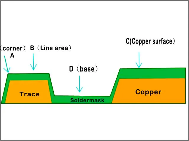
The solder mask interacts with the PCB substrate and copper features through adhesion and thermal expansion characteristics. During reflow processes, the coating must withstand elevated temperatures without delaminating or cracking, which preserves the underlying copper integrity. Color variations in the solder mask affect heat absorption and reflection, influencing localized thermal gradients during assembly and operation. Darker colors tend to absorb more thermal energy, potentially accelerating material aging in high-power designs, while lighter colors dissipate heat more readily. Solder mask clearance around pads and traces determines the extent of copper exposure, affecting both solder fillet formation and insulation resistance between conductors. These mechanisms collectively shape the board response to mechanical flexure and moisture ingress.

Practical Solutions and Best Practices
Designers specify solder mask requirements early in the layout process to align with assembly needs and reliability targets. Adequate clearance between the mask edge and pad perimeter ensures reliable solder wetting without mask encroachment that could impede joint formation. Application methods must achieve uniform thickness to avoid thin spots that compromise insulation or thick areas that trap contaminants. Selection of solder mask color balances visual inspection needs with thermal performance considerations in the intended environment. Collaboration between design and manufacturing teams verifies that the chosen mask type meets adhesion and hardness criteria under expected thermal cycling. Regular review of design rules for mask registration tolerances minimizes defects that could propagate into field failures.
Impact on PCB Reliability
Reliability testing often evaluates how the outer layer solder mask performs under combined thermal, humidity, and electrical stresses. A well-applied mask enhances resistance to electrochemical migration by limiting moisture pathways to copper surfaces. In contrast, defects such as pinholes or poor adhesion create entry points for contaminants that accelerate corrosion and increase leakage currents. The mask also contributes to mechanical protection against handling damage and vibration-induced wear during product life. Standards such as those from IPC define performance classes that differentiate requirements for commercial versus high-reliability end uses. Consistent mask quality across production lots supports predictable mean time between failures in deployed systems.
Conclusion
The outer layer solder mask represents a foundational element in achieving desired PCB performance and reliability outcomes. Its influence spans electrical isolation, thermal management, and environmental protection when properly specified and applied. Engineers achieve optimal results by integrating mask considerations into the overall design workflow rather than treating them as a secondary manufacturing step. Attention to clearance, color, and material class supports consistent assembly yields and extended product life. Ongoing adherence to established qualification practices ensures that boards meet the demands of their target applications.
FAQs
Q1: How does solder mask clearance affect PCB assembly and reliability?
A1: Solder mask clearance defines the gap between the mask edge and exposed copper features such as pads. Adequate clearance promotes complete solder wetting during reflow while preventing mask material from interfering with joint formation. Insufficient clearance can lead to incomplete solder fillets or trapped flux residues that compromise long-term electrical performance. Proper clearance specification therefore supports both manufacturing yield and field reliability of the assembled board.
Q2: What role do solder mask colors play in PCB outer layer solder mask performance?
A2: Solder mask colors influence thermal behavior during soldering and operation because different pigments absorb or reflect heat at varying rates. Lighter colors generally reduce heat buildup in high-power or densely populated boards, while darker colors may require additional thermal management considerations. Color choice also affects automated optical inspection contrast and manual visual checks during quality control. Selecting an appropriate color aligns visual and thermal requirements with the overall reliability goals of the design.
Q3: Why is solder mask application critical for PCB reliability?
A3: Solder mask application creates a uniform protective barrier that shields copper from oxidation, moisture, and chemical exposure throughout the product lifecycle. Uniform coverage and adhesion prevent localized failures such as corrosion or delamination that can initiate under thermal cycling or humidity stress. Consistent application processes ensure that insulation resistance remains stable and that solder bridging risks stay minimized during assembly. These factors collectively determine whether the finished PCB maintains functionality over its intended service life.
Q4: How do industry standards guide solder mask selection for high-reliability PCBs?
A4: Standards such as IPC-SM-840 establish qualification requirements for permanent solder mask materials, including tests for adhesion, dielectric strength, and environmental resistance. These specifications differentiate performance classes suited to commercial or more demanding applications. Compliance helps ensure that the mask maintains its protective and insulating properties after multiple thermal excursions and prolonged exposure to operating conditions. Designers reference such standards to verify material suitability before committing to production.
References
[1] The Inseparable Connection: Solder Mask Color and PCB Reliability
[2] NCAB Group: PCB Solder Mask
IPC-SM-840 — Qualification and Performance of Permanent Solder Mask. IPC
IPC-6012 — Qualification and Performance Specification for Rigid Printed Boards. IPC
IPC-A-600 — Acceptability of Printed Boards. IPC


