 ALLPCB


Introduction
Electric vehicle charging infrastructure continues to expand rapidly as adoption of EVs increases worldwide. This growth places new demands on printed circuit boards used in charging stations and related equipment. PCBs in these systems must manage high currents, elevated voltages, and significant thermal loads while maintaining long-term reliability. Engineers designing these boards focus on material selection, layout strategies, and compliance with established performance criteria to ensure safe operation. The integration of power electronics with control circuitry further complicates the design process, requiring careful attention to isolation and signal integrity.
Why PCB Design Matters for EV Charging Stations
EV charging stations operate at power levels ranging from several kilowatts in residential units to hundreds of kilowatts in fast chargers. These conditions require PCBs capable of handling continuous high-current flow without excessive heating or degradation. Standard consumer electronics boards often fall short in such environments, leading designers to adopt specialized approaches for trace widths, copper weights, and layer stacking. Effective PCB design directly influences charging efficiency, system uptime, and overall safety margins. As infrastructure scales, the role of robust board-level engineering becomes central to meeting performance expectations across diverse installation sites.
Technical Principles of High-Power PCB Design
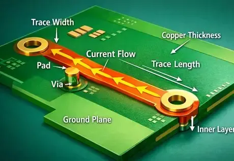
High-power PCB design for EV chargers centers on managing current density and minimizing resistive losses. Engineers increase copper thickness and optimize trace geometry to keep temperatures within acceptable limits during prolonged operation. Multilayer constructions often incorporate dedicated power planes alongside signal layers to separate high-voltage domains from sensitive control circuits. Thermal vias and strategic component placement help conduct heat away from critical areas such as power semiconductors and connectors. These principles derive from fundamental electrical and thermal engineering considerations rather than ad-hoc adjustments.
Thermal Management Approaches
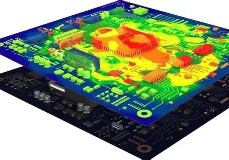
Thermal management remains a primary concern because power conversion stages generate substantial heat. Designers evaluate the use of metal-core substrates or enhanced dielectric materials to improve heat spreading across the board. Proper via stitching and heatsink attachment points further aid dissipation when airflow or liquid cooling is available at the system level. Simulation of steady-state and transient thermal profiles guides layout decisions before prototyping. Attention to these factors helps prevent localized overheating that could affect component lifespan or trigger protective shutdowns.
Safety and Insulation Requirements
Safety considerations dictate minimum distances for creepage and clearance to prevent arcing or insulation breakdown under high-voltage conditions. These distances scale with operating voltage and environmental factors such as pollution degree and altitude. Standards such as those from the IEC provide guidance on insulation coordination that designers apply when defining board geometries and material properties. Proper selection of solder mask and conformal coatings adds another layer of protection in humid or contaminated environments. Consistent application of these rules supports reliable performance over the service life of the charger.
PCB Considerations for Wireless EV Charging
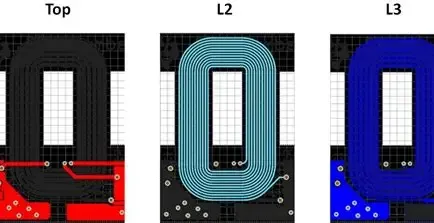
Wireless EV charging systems introduce additional PCB requirements centered on coil integration and electromagnetic compatibility. Resonant coils are often realized as planar structures on dedicated board layers or as separate assemblies connected to the main PCB. Precise control of inductance, capacitance, and quality factor becomes essential for efficient power transfer across an air gap. Shielding layers and careful routing help contain magnetic fields and reduce interference with nearby electronics. These designs must also accommodate alignment tolerances and foreign-object detection features without compromising thermal or electrical performance.
Best Practices and Design Guidelines
Engineers follow structured design flows that begin with power budget analysis and progress through schematic capture, layout, and verification. Early collaboration between electrical and mechanical teams ensures adequate space for cooling provisions and mechanical mounting. Use of thicker copper foils, selective heavy-copper plating, and reinforced via structures addresses current-carrying needs while maintaining manufacturability. Regular design reviews against qualification criteria help identify potential issues before fabrication. Documentation of thermal and electrical margins supports traceability and future design iterations.
Standards such as IPC-6012E inform qualification and performance expectations for rigid boards used in these demanding applications. Reference to such documents occurs at appropriate stages rather than repeatedly throughout the process.
Conclusion
EV charging infrastructure imposes distinct requirements on PCB design that extend beyond conventional electronics practices. High current handling, thermal dissipation, and insulation coordination form the core challenges that engineers address through material choices, layout techniques, and compliance with recognized standards. Wireless implementations add further complexity around coil integration and field management. Systematic application of established engineering principles yields boards that support safe, efficient, and durable charging systems. Continued refinement of these approaches will remain important as power levels and deployment volumes increase.
FAQs
Q1: What are the main challenges when designing PCBs for EV charging stations?
A1: High current capacity, effective heat removal, and adequate electrical isolation represent the primary challenges. Designers must balance trace dimensions and copper thickness against board size and cost constraints while ensuring compliance with performance specifications. Thermal management often requires additional features such as metal cores or enhanced via structures. These considerations apply across both conductive and wireless charging architectures.
Q2: How does thermal management affect PCB reliability in high-power EV chargers?
A2: Excessive temperature rise accelerates material aging and can shift electrical characteristics of components and traces. Proper thermal paths, including strategic via placement and substrate selection, keep operating temperatures within safe limits. This approach supports consistent performance over thousands of charging cycles. Engineers verify designs through simulation and testing to confirm adequate margins.
Q3: What PCB safety standards apply to EV charging equipment?
A3: Designers reference IEC guidelines for insulation coordination and clearance distances appropriate to the operating voltage and environment. IPC-6012E provides qualification criteria for the rigid boards themselves. These documents help establish consistent safety margins without prescribing specific product implementations.
Q4: Are there special considerations for PCBs used in wireless EV charging systems?
A4: Wireless systems require precise control of planar coil parameters and electromagnetic shielding to achieve efficient power transfer. The PCB must accommodate both power delivery and control functions while managing magnetic fields and potential interference. Alignment with overall system efficiency goals influences layer stack-up and material choices.
References
IPC-6012E — Qualification and Performance Specification for Rigid Printed Boards. IPC, 2017
IEC 60664-1 — Insulation Coordination for Equipment within Low-Voltage Systems. IEC, 2020


