 ALLPCB


The Impact of Black Silkscreen on PCB Testing and Debugging
Black silkscreen layers on printed circuit boards serve as the legend that identifies component locations, polarity markers, test points, and reference designators. When black ink is selected instead of the more common white or yellow, the contrast against typical solder mask colors and copper features changes significantly. This choice influences how easily technicians locate measurement locations during PCB testing and how quickly they can interpret markings while performing PCB debugging. Engineers working on high-density boards often encounter situations where reduced visibility extends troubleshooting time or increases the chance of probing the wrong node. Understanding these effects helps design teams balance aesthetic or functional requirements with the practical needs of verification and repair workflows.
Why Black Silkscreen Visibility Matters for PCB Testing
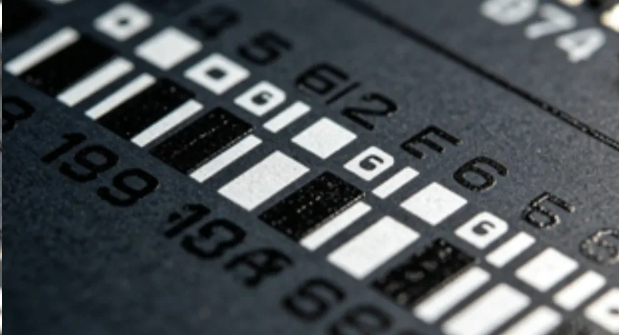
The primary role of silkscreen during PCB testing is to guide probe placement and confirm that measurements occur at the intended circuit nodes. Black silkscreen reduces contrast when applied over dark solder masks or near black components, making small text and symbols harder to read under standard bench lighting. In contrast, white or yellow legends remain legible across a wider range of background colors and lighting conditions. This visibility difference directly affects test point identification, especially on boards that undergo repeated measurements or environmental stress testing. Procurement and design teams therefore evaluate silkscreen color early in the layout phase to avoid downstream delays in PCB troubleshooting.
Technical Principles of Silkscreen and Solder Mask Interaction
Silkscreen ink is applied after solder mask curing and must maintain adhesion and legibility through subsequent assembly and handling steps. Industry standards such as IPC-A-600 define visual acceptability criteria for legend clarity and contrast. When black ink is used, its reflectance properties can cause the printed characters to blend with dark solder mask surfaces, particularly under diffuse lighting typical of laboratory environments. Copper traces and pads already present low-contrast areas; adding black legend further reduces the differentiation needed for rapid visual location of test points. Thermal expansion differences between ink and substrate can also cause minor cracking or fading over time, though this remains within acceptable limits when IPC-6012 qualification requirements are followed.
Effects on Test Point Identification and PCB Debugging Workflows
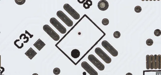
During manual probing or automated test fixture setup, technicians rely on silkscreen to align probes quickly and avoid adjacent pads that could cause shorts. Black legend markings become difficult to distinguish when the board is populated with dark IC packages or when conformal coating is later applied. This situation lengthens the time required to isolate faults during PCB debugging sessions, especially on multilayer boards where via locations must also be verified. In high-volume production environments, extended debug cycles translate into higher labor costs and potential schedule slippage. Structured test procedures that include photographs or coordinate maps can mitigate some of these issues, yet the fundamental visibility limitation remains tied to the chosen silkscreen color.

Best Practices for Design and Testing with Black Silkscreen
Design teams can maintain adequate test point visibility by increasing font sizes for critical reference designators and by placing test points on areas with lighter solder mask or exposed copper where contrast improves. Adding supplementary fiducial marks or using a hybrid silkscreen approach, such as white text on selected high-priority zones, provides redundancy without changing the overall board appearance. During PCB testing, technicians benefit from consistent use of magnification tools and adjustable lighting that emphasizes edge definition rather than relying solely on color contrast. Documentation packages should include both silkscreen drawings and separate test point coordinate lists so that visibility limitations do not impede verification activities. These measures align with the quality expectations outlined in IPC-6012 for rigid printed boards.
Conclusion
Black silkscreen offers certain aesthetic or functional advantages on specific PCB designs yet introduces measurable challenges for test point identification and efficient PCB debugging. By understanding the interaction between legend color, solder mask, and lighting conditions, engineering teams can implement targeted layout adjustments and procedural safeguards. Adherence to established standards such as IPC-A-600 ensures that visual quality remains acceptable while supporting reliable PCB testing throughout the product lifecycle. Early consideration of these factors during the design review process reduces the risk of extended troubleshooting and supports consistent manufacturing outcomes.
FAQs
Q1: How does black silkscreen affect PCB testing compared with white silkscreen?
A1: Black silkscreen reduces contrast against dark solder masks and components, making test point identification more difficult under typical laboratory lighting. White silkscreen maintains higher visibility across most background colors, allowing faster probe placement during PCB testing. Engineers often compensate by enlarging critical markings or adding coordinate documentation when black legend is required.
Q2: What steps improve test point visibility on boards that use black silkscreen?
A2: Increasing font size for reference designators, selecting lighter solder mask in test areas, and providing separate test point maps all help maintain efficient PCB debugging. Consistent use of magnification and directional lighting further assists technicians in locating measurement nodes despite reduced color contrast.
Q3: Does black silkscreen comply with industry standards for PCB quality?
A3: Black silkscreen is acceptable under IPC-A-600 visual criteria provided the legend remains legible and properly adhered. Boards must still meet the qualification requirements of IPC-6012 for rigid printed boards, which address both electrical performance and visual attributes regardless of legend color.
Q4: Can black silkscreen increase the time needed for PCB troubleshooting?
A4: Yes, lower contrast can extend the duration of manual probing and fault isolation because technicians spend additional time confirming locations. Structured test procedures and supplementary documentation help limit these delays while preserving the design intent behind the black silkscreen choice.
References
IPC-A-600K - Acceptability of Printed Boards. IPC, 2020
IPC-6012E - Qualification and Performance Specification for Rigid Printed Boards. IPC, 2017





