 ALLPCB


Multilayer printed circuit boards rely on carefully chosen copper thicknesses for inner layers to support reliable electrical performance and manufacturability. Inner layer copper thickness directly influences impedance control, current carrying capacity, and heat dissipation in complex designs. Engineers often describe the ideal selection as a Goldilocks zone, where the thickness meets functional needs without unnecessary material or processing costs. This balance becomes especially important in high speed digital, power, and mixed signal boards where signal integrity and thermal management must coexist.
Why Inner Layer Copper Thickness Matters in PCB Design
Inner layers in multilayer boards carry signals, power, and ground planes that determine overall system behavior. Selecting copper weight too thin can increase resistance and voltage drop, while excessive thickness raises material costs and complicates etching processes. The choice affects trace width requirements for a given current, impedance targets for high speed signals, and the ability to manage localized heating. Industry specifications such as IPC 6012E establish qualification criteria that help ensure inner layer copper meets performance and reliability expectations across production volumes.
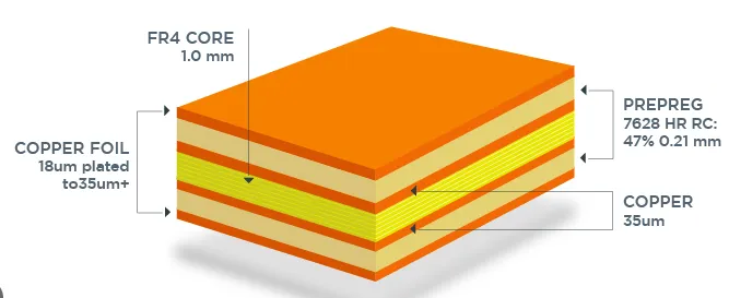
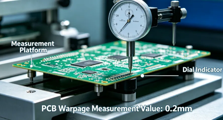
Design teams evaluate copper thickness early in the stackup definition because changes later affect layer count, dielectric spacing, and overall board thickness. Thinner copper on signal layers supports finer features and tighter impedance control, whereas power planes often benefit from heavier copper to reduce IR drop. Thermal performance improves with increased copper cross section, yet this must be weighed against manufacturing yield and board warpage risks during lamination and reflow. Proper selection therefore supports both electrical and mechanical stability throughout the product lifecycle.
Technical Principles Governing Copper Thickness Selection
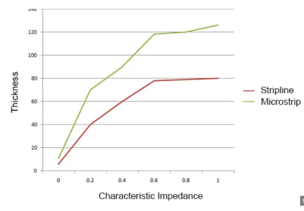
Copper thickness determines the resistance per unit length of a trace according to the relationship R equals rho times L over A, where A is the cross sectional area. For inner layers, this resistance influences both DC power distribution and high frequency signal attenuation. At radio frequencies, skin effect concentrates current near the conductor surface, so very thick copper provides diminishing returns for signal integrity while still adding cost and weight. Controlled impedance calculations incorporate copper thickness as a variable that interacts with trace width, dielectric constant, and height above the reference plane.
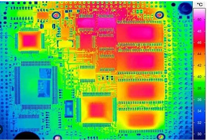
Heat transfer follows Fourier's law, with thicker copper offering lower thermal resistance along the plane. In boards with high power dissipation, this helps spread heat away from components, yet excessive copper can create thermal gradients that contribute to warpage if the stackup is not symmetric. IPC A 600K provides acceptability criteria for copper thickness uniformity and surface quality that directly relate to these electrical and thermal considerations. Designers therefore model both electrical and thermal behavior using the same copper thickness parameter to identify the zone where performance targets are met efficiently.
Signal integrity concerns such as crosstalk and return path integrity also scale with copper geometry. Thinner inner layer copper allows closer spacing of differential pairs while maintaining target impedance, but it increases resistive losses that can degrade eye diagrams at multi gigabit rates. Conversely, heavier copper reduces losses yet may require wider traces or adjusted dielectric thicknesses to achieve the same impedance, potentially increasing board size or layer count. The interplay of these factors leads engineers to iterate stackup options until the chosen inner layer copper satisfies all constraints simultaneously.
Practical Guidelines for Selecting Optimal Inner Layer Copper Thickness
Begin by defining the primary functions of each inner layer: high speed signals, power distribution, or ground reference. For signal layers, start with 0.5 ounce or 1 ounce copper to enable fine line etching and precise impedance control. Power and ground planes frequently use 1 ounce or 2 ounce copper to minimize voltage drop under expected load currents. Reference IPC 6012E when establishing minimum copper thickness and uniformity requirements for the intended board class.
Next, perform current carrying capacity calculations using established methods that account for temperature rise limits. Adjust trace widths accordingly and verify that the resulting geometry fits within available routing channels. Thermal simulations can then confirm that the chosen copper thickness adequately spreads heat without creating hot spots that exceed component ratings. When high speed signals dominate, run impedance and loss simulations across the expected frequency range to confirm the thickness supports required margins.
Finally, review the complete stackup for symmetry and manufacturability. Asymmetric copper distribution increases the risk of warpage during thermal cycling, so balance copper weights on opposite sides of the core. Consult fabrication notes for minimum finished copper tolerances and plating requirements. This structured approach consistently identifies the Goldilocks thickness that satisfies electrical, thermal, and cost objectives without overdesign.
Balancing Trade offs in Real World Designs
In practice, signal integrity requirements often favor thinner copper on inner signal layers, while power integrity pushes toward heavier copper on planes. When both coexist on the same board, hybrid stackups with selective copper weights become necessary. Cost considerations include raw material, etching time, and yield impact from finer features on thicker copper. Thermal performance gains from added copper must be validated against the added weight and potential mechanical stress.
Design reviews should include sensitivity analysis around copper thickness tolerances. Small deviations from nominal thickness can shift impedance outside acceptable windows or increase resistive losses beyond simulation predictions. Documenting the rationale for each layer's copper weight supports future revisions and supplier communication. This documentation also helps procurement teams align material specifications with the intended performance targets.
Conclusion
Selecting the optimal inner layer copper thickness requires systematic evaluation of electrical, thermal, and manufacturing factors. The Goldilocks zone emerges when the chosen weight satisfies impedance targets, current demands, and heat spreading needs without excess material or processing difficulty. Adherence to IPC 6012E and IPC A 600K provides the qualification framework that supports consistent results across production. Engineers who apply these principles early in the design cycle achieve reliable boards that meet performance goals efficiently.
FAQs
Q1: What copper thickness is typically recommended for inner signal layers in high speed PCB designs?
A1: One half ounce or one ounce copper is commonly selected for inner signal layers because it supports fine line etching and precise impedance control while keeping resistive losses manageable. This choice aligns with signal integrity requirements in most digital and RF applications without driving unnecessary cost or manufacturing complexity.
Q2: How does inner layer copper thickness affect thermal performance in power dense PCBs?
A2: Thicker copper increases the cross sectional area available for heat spreading, which lowers thermal resistance along the plane and helps reduce localized temperature rise. Designers balance this benefit against potential increases in board weight and warpage risk when specifying copper weights for power and ground layers.
Q3: Why is balancing copper thickness important for signal integrity versus cost in multilayer boards?
A3: Thinner copper enables tighter impedance control and finer features that support high speed signaling, yet it can raise resistive losses and voltage drop. Heavier copper reduces these electrical penalties but increases material expense and may require wider traces, so the optimal thickness meets both performance and budget constraints simultaneously.
Q4: What role do industry standards play when specifying inner layer copper thickness?
A4: Standards such as IPC 6012E define qualification and performance requirements for copper thickness, uniformity, and acceptability that help ensure the finished board meets reliability targets. Following these guidelines reduces the risk of manufacturing defects and supports consistent results across suppliers.
References
IPC-6012E - Qualification and Performance Specification for Rigid Printed Boards. IPC, 2017
IPC-A-600K - Acceptability of Printed Boards. IPC, 2020


