 ALLPCB


Why Matte Finishes Matter in Modern PCB Production
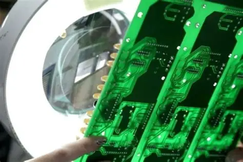
Matte solder mask finishes feature a non-reflective, textured surface that appears darker and softer compared to glossy alternatives. This texture arises from controlled surface roughness during the curing and application process. In factory settings, the choice between matte and glossy directly influences inspection efficiency and assembly yields. Manufacturers often select matte finishes when automated optical inspection systems or manual visual checks play a central role in quality control. The reduced glare improves contrast, allowing defects such as misalignments or contamination to stand out more clearly.
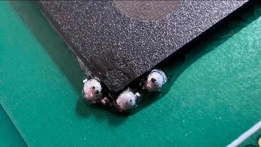
Industry standards guide these decisions to ensure consistent performance across production runs. IPC-SM-840 outlines qualification and performance requirements for solder mask materials, including adhesion, hardness, and resistance to soldering processes. Matte finishes can contribute to better process reliability in reflow soldering environments by influencing how molten solder interacts with the surface. Surface roughness tends to promote a convex meniscus that limits solder ball adhesion compared to smoother glossy surfaces. This characteristic supports higher first-pass yields in high-volume manufacturing.

Technical Principles Behind Matte Solder Mask Performance
The engineering mechanisms of matte finishes center on surface topography and its interaction with light, solder, and inspection equipment. Roughness scatters incident light rather than reflecting it specularly, which minimizes hotspots that can obscure fine features during automated or manual inspection. In high-density interconnect boards, this property becomes especially valuable because trace spacing and pad geometries continue to shrink. The same roughness affects wetting behavior during soldering, where the altered meniscus formation can reduce the incidence of stray solder balls that might otherwise cause shorts or rework.
Next-generation solder mask materials build on these principles by incorporating advanced polymer formulations designed for improved thermal stability and mechanical durability. These developments address the needs of applications involving higher operating temperatures or repeated thermal cycling. Factory processes for applying such materials often involve liquid photoimageable inks or dry-film options optimized for laser direct imaging to achieve precise feature definition on matte surfaces. The result supports tighter tolerances while maintaining the inspection benefits of the finish.
Advanced solder mask technology also explores ways to enhance compatibility with emerging assembly techniques. For instance, the textured surface can improve adhesion for subsequent conformal coatings or underfills in certain assemblies. Manufacturers evaluate these properties through standardized testing protocols that verify performance under environmental stress. Such evaluations help ensure that the solder mask maintains integrity without introducing new failure modes in the final product.
Best Practices for Implementing Matte Finishes
Procurement and design teams should specify matte finishes early in the layout phase when inspection or solderability concerns predominate. Clear documentation of finish type helps fabricators select appropriate ink formulations and curing parameters. In practice, this means reviewing board density, expected assembly processes, and end-use environment before finalizing the solder mask callout. Collaboration between design and manufacturing engineers reduces the likelihood of downstream issues such as excessive glare or inconsistent coverage.
Quality control procedures benefit from the inherent visibility advantages of matte surfaces. Automated systems require less specialized lighting calibration, and human inspectors experience reduced eye strain during extended reviews. When combined with appropriate panel handling protocols, these finishes contribute to lower defect escape rates. Engineers also consider thickness uniformity, because variations can affect both electrical performance and the visual characteristics of the matte appearance.
For applications pushing the boundaries of current technology, evaluation of next-generation solder mask materials includes assessments of long-term reliability under accelerated life testing. This approach helps identify formulations that maintain the desirable matte properties while meeting evolving thermal and chemical resistance demands. Documentation of these evaluations supports traceability and continuous improvement in production environments.
Emerging Directions in Advanced Solder Mask Technology
Future PCB trends point toward materials that combine the proven benefits of matte finishes with enhanced functional properties. Research into advanced polymeric systems aims to deliver improved resistance to thermal shock and better compatibility with high-frequency signals. Some development efforts focus on incorporating features that could respond dynamically to environmental changes, representing early steps toward what might be described as smart solder mask concepts. These innovations remain grounded in the need for manufacturability at scale.
Self-healing solder mask represents another area of interest in next-generation solder mask materials, where polymer chemistry could potentially repair minor surface damage over time. While still largely in exploratory stages, such capabilities would align with sustainability goals by extending board service life. Manufacturers monitor these developments closely because any new material must integrate seamlessly with existing imaging, development, and curing equipment. Pilot production runs help validate performance before broader adoption.
Thermal management continues to drive material selection, with matte finishes offering additional benefits in heat dissipation scenarios due to their surface characteristics. As power densities rise in automotive, aerospace, and computing applications, the ability to maintain stable electrical and mechanical properties under elevated temperatures becomes critical. Standards such as those in the IPC-6012 series provide the framework for qualifying boards that incorporate these advanced finishes.
Conclusion
Matte solder mask finishes deliver tangible advantages in inspection visibility and assembly process control that support high-reliability PCB manufacturing. Continued evolution in material science promises further enhancements through advanced solder mask technology and next-generation solder mask materials. Engineers who align design choices with factory capabilities and relevant industry standards position their projects for success in increasingly complex applications. These trends underscore the ongoing importance of surface finish selection in achieving both performance and producibility goals.
FAQs
Q1: What advantages does matte solder mask offer compared to glossy finishes in advanced solder mask technology?
A1: Matte finishes provide superior inspection visibility by eliminating glare and improving contrast for both manual and automated systems. The textured surface can also reduce solder ball formation during reflow processes, supporting higher assembly yields. These characteristics make matte options particularly suitable for high-density designs where defect detection is essential.
Q2: How might self-healing solder mask contribute to future PCB trends?
A2: Self-healing concepts in next-generation solder mask materials explore polymer systems that could address minor surface imperfections autonomously. This capability would enhance long-term reliability in demanding environments. Development focuses on maintaining compatibility with standard manufacturing processes while adding resilience.
Q3: What role do smart solder mask features play in next-generation solder mask materials?
A3: Smart solder mask approaches investigate materials with responsive properties, such as improved thermal regulation or environmental sensing. These advancements aim to meet the requirements of increasingly complex electronic systems. Integration must preserve the core protective functions while adding value in specific applications.
Q4: Why are industry standards important when specifying matte finishes for advanced solder mask technology?
A4: Standards such as IPC-SM-840 and IPC-6012 establish consistent requirements for material performance, adhesion, and environmental resistance. They guide manufacturers in qualifying processes and verifying that finishes meet reliability targets. Proper adherence ensures compatibility across the supply chain and supports quality outcomes.
References
IPC-SM-840 — Qualification and Performance Specification of Permanent Solder Mask and Flexible Cover Materials. IPC
IPC-6012E — Qualification and Performance Specification for Rigid Printed Boards. IPC, 2017
IPC-A-600K — Acceptability of Printed Boards. IPC, 2020


