 ALLPCB


Lead-free solder has become a standard choice in electronics manufacturing because it supports environmental goals while meeting performance requirements for modern assemblies. In flex PCB applications, where thin substrates and dynamic bending are common, the transition from traditional tin-lead alloys requires careful attention to material compatibility and process parameters. Electrical engineers often evaluate these solders for their ability to reduce hazardous substances without compromising joint integrity. Sustainable assembly practices now emphasize compliance with global regulations that restrict lead content, driving adoption across consumer, automotive, and industrial sectors.
Why Lead-Free Solder Matters for Sustainable Flex PCB Assembly
Sustainable assembly in flex PCB production focuses on minimizing environmental impact throughout the product lifecycle. Lead-free solder, typically based on tin-silver-copper compositions, eliminates lead while maintaining electrical conductivity and mechanical strength. This shift aligns with broader industry efforts to create eco friendly solder pcb options that support recycling and reduce toxicity in end-of-life disposal. Engineers working on flexible circuits appreciate how these alloys enable compliance without requiring entirely new substrate materials in many cases. The result is assemblies that meet both performance specifications and sustainability targets.
Technical Principles of Lead-Free Soldering on Flexible Substrates
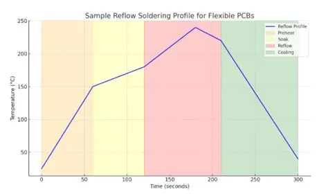
Lead-free solders generally exhibit higher melting points than tin-lead alternatives, often requiring reflow profiles that peak between 240 and 260 degrees Celsius. This temperature range demands precise control to avoid damaging the polyimide or polyester films used in flex circuits. Higher reflow temperatures can increase the risk of substrate warpage or delamination if the process is not optimized for the specific stack-up. Joint formation relies on proper wetting and intermetallic compound growth, which differs from leaded solders due to the absence of lead's influence on surface tension.
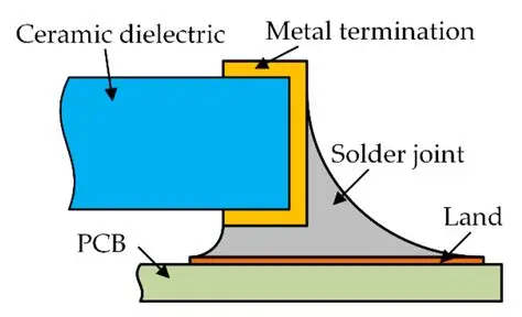
Engineers must also consider the coefficient of thermal expansion mismatch between the solder, copper traces, and flexible dielectric. This mismatch becomes more pronounced during thermal cycling, potentially leading to fatigue in dynamic flex applications. Standards such as those from IPC provide guidelines for evaluating solder alloy performance under these conditions. Alternative lead solder formulations continue to evolve, with additions like bismuth or antimony helping to lower melting points and improve reliability in certain flex designs.
Related Reading: Lead Solder vs Lead-Free Solder: Which One Should You Choose
Best Practices for Lead-Free Implementation in Flex PCB Assembly
Successful adoption of rohs compliant solder begins with thorough process characterization on the specific flex materials in use. Reflow oven profiling should account for the thermal mass of the assembly and the sensitivity of components mounted on the flexible sections. Stencil design and solder paste volume require adjustment because lead-free pastes often exhibit different slump and tack properties compared with leaded versions.
Related Reading: A Step by Step Guide to Lead Free Solder Paste Application for Beginners
Post-assembly inspection benefits from updated acceptance criteria that recognize the distinct appearance of lead-free joints, including their typically duller surface finish. Engineers frequently perform thermal cycling and bend testing to verify long-term performance in applications involving repeated flexing. Maintaining consistent nitrogen atmosphere during reflow can further improve wetting and reduce oxidation risks associated with higher process temperatures.
Addressing Common Challenges in Lead-Free Flex Assembly
One frequent issue involves increased voiding in solder joints when using lead-free pastes on flex substrates with limited thermal conductivity. Mitigation often includes optimizing paste formulation, adjusting reflow soak times, and ensuring proper outgassing paths in the stencil design. Another consideration is the potential for head-in-pillow defects with area-array components, which can be reduced through improved component placement accuracy and flux activity matching.
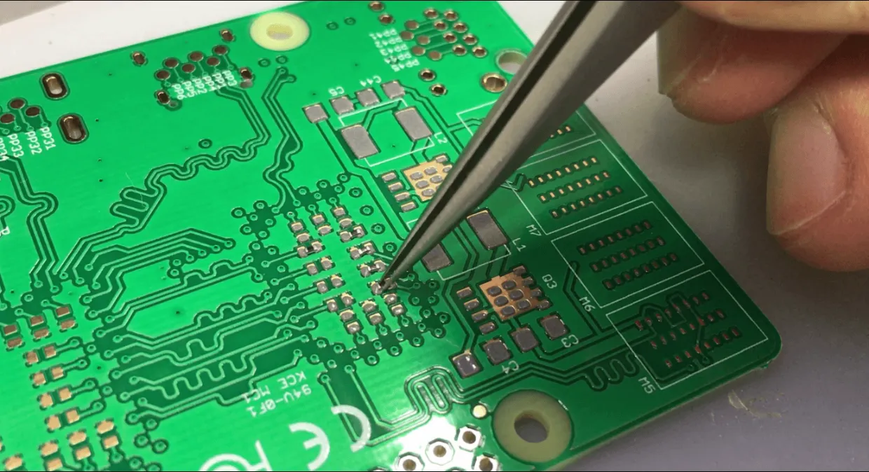
Troubleshooting also extends to rework scenarios, where localized heating must avoid overheating adjacent flex areas. Engineers typically document process windows that balance joint quality with substrate integrity, drawing on established industry practices for consistent results across production lots.
Conclusion
Lead-free solder enables sustainable assembly practices in flex PCB manufacturing by reducing environmental hazards while supporting reliable electronic performance. Through careful attention to thermal profiles, material interactions, and inspection methods, engineers can achieve high-quality outcomes that meet both regulatory and functional demands. Continued refinement of alternative lead solder alloys promises further improvements in process windows and long-term durability for flexible circuit applications.
FAQs
Q1: What are the main advantages of using lead free solder in flex PCB production?
A1: Lead free solder supports regulatory compliance and reduces environmental impact while providing adequate mechanical and electrical performance for most flexible circuit applications. Engineers select these alloys to align with sustainable assembly goals without major redesigns in many cases.
Q2: How does rohs compliant solder affect the assembly process for flexible circuits?
A2: Rohs compliant solder typically requires higher reflow temperatures, which engineers manage through adjusted profiles and material selection to prevent damage to thin flex substrates. Proper process controls help maintain joint reliability comparable to traditional options.
Q3: Are there reliable eco friendly solder pcb alternatives to traditional lead-based materials?
A3: Yes, tin-silver-copper and related formulations serve as effective eco friendly solder pcb options that meet performance standards when processes are optimized for flex applications. These alternatives continue to improve through alloy refinements.
Q4: What testing helps verify lead-free solder performance on dynamic flex assemblies?
A4: Thermal cycling, bend endurance, and shear testing provide data on joint durability under conditions typical of flexible circuit use. Such evaluations confirm that the chosen lead free solder meets application-specific requirements.
References
IPC J-STD-006C — Requirements for Electronic Grade Solder Alloys and Fluxed and Non-Fluxed Solid Solders for Electronic Soldering Applications. IPC, 2013
IPC-A-610H — Acceptability of Electronic Assemblies. IPC, 2020
JEDEC J-STD-020F — Moisture/Reflow Sensitivity Classification for Nonhermetic Surface Mount Devices. JEDEC, 2022





