 ALLPCB


Introduction
In the fast-paced world of electronics manufacturing, PCB panelization stands as a cornerstone for optimizing production efficiency and reducing costs. For electrical engineers tackling heterogeneous PCB panelization, the challenge intensifies when dealing with mixed PCB designs panel that incorporate boards of varying sizes, shapes, and functionalities. This DFM approach ensures that combining different PCB types panel becomes not just feasible but strategically advantageous, maximizing material utilization while adhering to tight tolerances. By thoughtfully arranging multiple boards on a single panel, manufacturers achieve economies of scale that single-board runs simply cannot match. This article delves into the principles, best practices, and engineering considerations that transform panelization into an art form, particularly for multi-project panelization scenarios. Understanding these elements empowers engineers to design panels that streamline fabrication, assembly, and depaneling processes.
What Is Heterogeneous PCB Panelization and Why It Matters
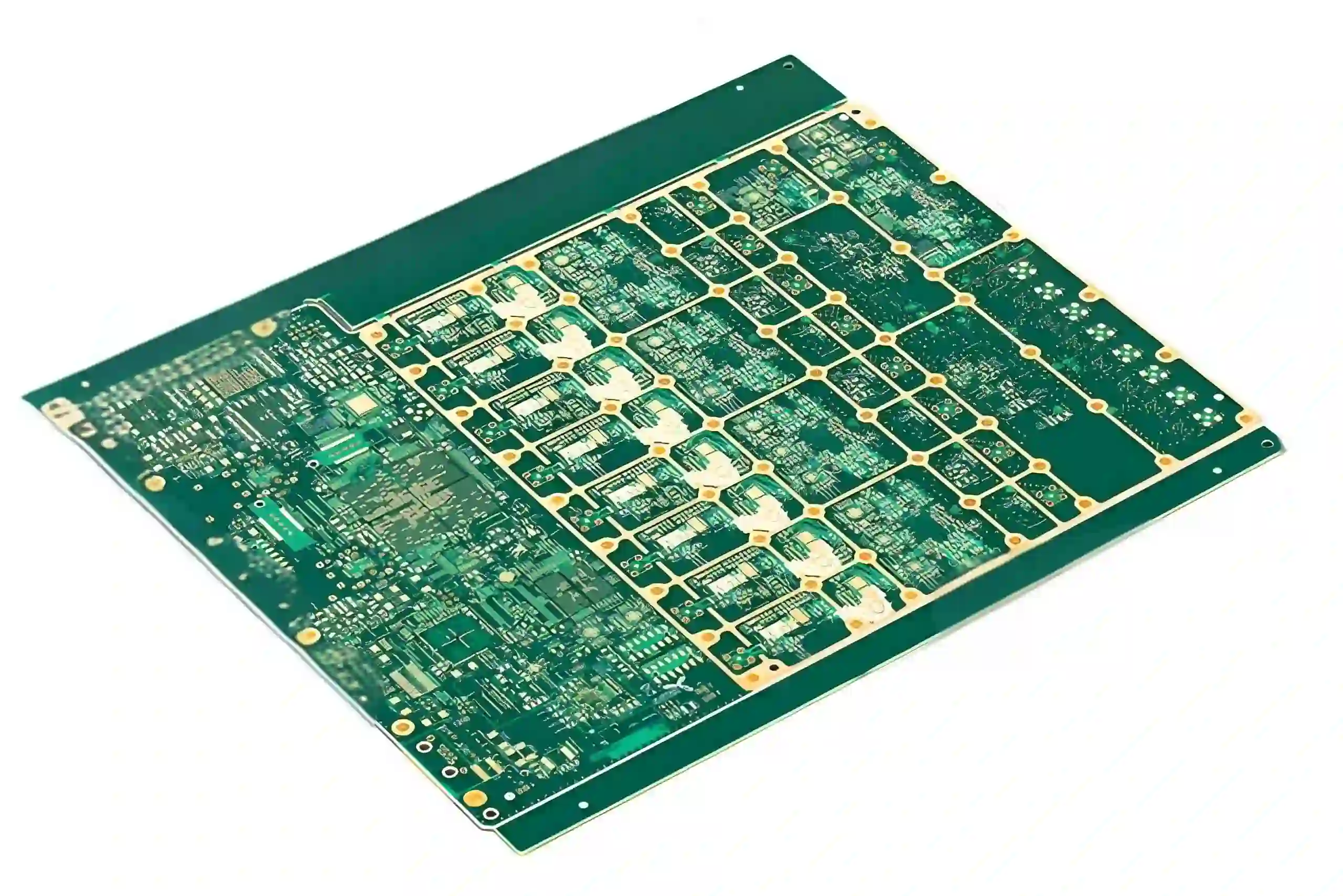
Heterogeneous PCB panelization refers to the process of grouping dissimilar printed circuit boards onto a unified panel for simultaneous manufacturing. Unlike uniform panels where all boards share identical dimensions and stackups, mixed PCB designs panel demand careful integration of boards with differing geometries, trace densities, and sometimes aspect ratios. This technique shines in scenarios like prototyping multiple variants or consolidating low-volume projects, directly addressing efficient material utilization panel goals. Industry relevance stems from its ability to cut down on setup times, minimize scrap, and enhance throughput in high-mix, low-volume environments common to R&D and custom electronics.
The economic impact is profound, as panelization reduces per-board costs by spreading fixed expenses across multiple units. For electrical engineers, mastering this means balancing design freedom with manufacturability constraints, ensuring that common layer stackup designs form the foundation for compatibility. Without proper planning, issues like uneven warpage or registration errors can cascade into yield losses, underscoring the DFM imperative. Ultimately, heterogeneous panelization bridges the gap between innovative design and practical production, fostering cost-effective mixed boards that accelerate time-to-market.
Technical Principles of Mixed PCB Panelization
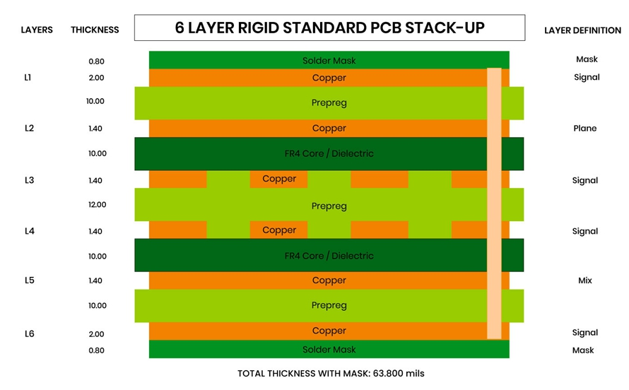
At its core, successful heterogeneous PCB panelization hinges on aligning board characteristics to a shared production framework, often centered around common layer stackup designs. Boards with matching layer counts, copper weights, and dielectric materials integrate seamlessly, as discrepancies in these parameters can lead to mismatched lamination pressures or thermal expansions during fabrication. Engineers must evaluate parameters like board thickness, typically standardized to increments of 0.1 mm or 0.2 mm, to prevent depaneling stresses that could fracture traces or vias. Fiducials, precisely placed tooling holes, serve as reference points for alignment, ensuring sub-micron accuracy across the panel array.
Material selection plays a pivotal role, with FR-4 or similar laminates preferred for their predictability in mixed arrays. Thermal coefficient of expansion (CTE) mismatches between boards can induce warpage, particularly post-reflow, so panels benefit from symmetric stackups that distribute stresses evenly. Routing strategies, such as tab routing or V-scoring, must account for varying board perimeters to avoid tab remnants that complicate depaneling. Adhering to IPC-2221 guidelines for printed board design helps mitigate these risks by promoting consistent drill sizes and pad geometries across the panel.
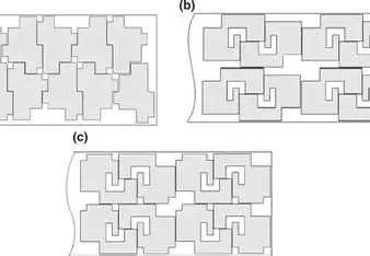
Panel yield optimization relies on statistical process control, where panel-level testing verifies impedance consistency and continuity before depaneling. For multi-project panelization, software algorithms simulate nesting to maximize board count per panel, factoring in keeper strips for edge support during handling. These principles ensure that combining different PCB types panel yields robust, high-reliability outcomes without compromising individual board performance.
DFM Best Practices for Cost-Effective Mixed Boards
Design for Manufacturability (DFM) elevates heterogeneous PCB panelization from a logistical exercise to a precision engineering strategy. Start by standardizing the panel outline to multiples of fabrication equipment capabilities, typically 18 x 24 inches or 20 x 22 inches, allowing efficient material utilization panel. Incorporate at least three fiducials per board, positioned asymmetrically to enable machine vision correction for rotation and scaling errors. For mixed PCB designs panel, group boards by similar impedance requirements to simplify etching processes and reduce recipe changes.
Optimized panel arrangement demands a nested layout that minimizes web widths between boards, usually 1.5 to 2 mm for routing tabs, while providing 5 mm borders for clamping. Electrical engineers should simulate warpage using finite element analysis, anticipating bow and twist limits per IPC-6012E specifications. Vias near panel edges require reinforcement to withstand depaneling forces, and ground planes should extend into breakaway areas for shielding during assembly. These practices directly contribute to cost-effective mixed boards by slashing material waste and non-conformance rates.
Depaneling method selection is critical: mouse bites suit irregular shapes in heterogeneous arrays, while scoring works for linear separations. Post-panelization inspections, including automated optical checks, confirm dimensional stability before singulation. By embedding these DFM rules early, engineers achieve multi-project panelization that scales production without proportional cost increases.
Challenges in Heterogeneous Panelization and Practical Solutions
One primary challenge in combining different PCB types panel is warpage, exacerbated by asymmetric copper distribution or CTE variances in mixed stackups. Solutions involve copper balancing, adding ground fills to lighter areas, and using carrier frames for thin boards during lamination. Another hurdle is registration accuracy, where drill-to-etch misalignment accumulates across the panel; counter this with direct imaging techniques and fiducial-based compensation.
Solder mask and silkscreen registration pose risks in high-density mixed designs, potentially leading to exposed traces. Factory-driven insights recommend over-etch margins and panel-level exposure to maintain tolerances. For assembly, ensure that BGA components on disparate boards align under shared reflow profiles, respecting JEDEC J-STD-020E moisture sensitivity classifications to prevent popcorn effects.
Troubleshooting often reveals depaneling-induced microcracks; mitigate with progressive routing paths and stress-relief slots. Yield data from panels guides iterative improvements, emphasizing the value of pilot runs for novel heterogeneous configurations. These targeted solutions transform potential pitfalls into opportunities for refined DFM.
Conclusion
Heterogeneous PCB panelization embodies the fusion of art and science in PCB manufacturing, where a DFM lens unlocks efficient material utilization panel and cost-effective mixed boards. By prioritizing common layer stackup designs, optimized panel arrangements, and rigorous adherence to standards like IPC-2221 and IPC-6012E, electrical engineers can navigate the complexities of mixed PCB designs panel with confidence. Multi-project panelization not only conserves resources but also accelerates innovation cycles, proving indispensable for modern electronics development. Embracing these principles ensures panels that deliver reliability, economy, and scalability, positioning designs for seamless transition from prototype to production.
FAQs
Q1: What are the key considerations for heterogeneous PCB panelization in multi-project environments?
A1: Heterogeneous PCB panelization requires matching layer stackups and material properties to enable combining different PCB types panel effectively. Focus on fiducial placement, minimal web widths, and warpage simulations to optimize yield. Adhering to DFM rules like symmetric copper distribution ensures efficient material utilization panel, reducing costs in low-volume runs. Standard inspections post-fabrication confirm compatibility before assembly.
Q2: How does optimized panel arrangement impact cost-effective mixed boards?
A2: Optimized panel arrangement maximizes board count per sheet, slashing per-unit fabrication expenses through better material utilization. Nest irregular shapes thoughtfully, maintaining 2 mm tabs and edge rails for handling stability. This approach suits mixed PCB designs panel by minimizing setup changes, with simulations guiding layouts for warpage control. Results include 20-40% cost savings typical in high-mix production.
Q3: What role do common layer stackup designs play in combining different PCB types panel?
A3: Common layer stackup designs provide the baseline for compatibility in heterogeneous panels, aligning dielectric thicknesses and copper foils. Variations in these lead to lamination voids or CTE mismatches, so standardize to 1.6 mm or 0.8 mm profiles. This facilitates multi-project panelization, ensuring uniform processing and high yields. Engineers verify via cross-sections during DFM reviews.
Q4: Can mixed PCB designs panel handle varying board thicknesses effectively?
A4: Yes, mixed PCB designs panel can accommodate slight thickness variations if compensated with carrier materials during pressing. Limit deltas to 0.1 mm and use symmetric builds per IPC guidelines. Depaneling methods like routing absorb stresses, with post-process checks for flatness. This maintains integrity for cost-effective mixed boards in diverse applications.


