ALLPCB


Introduction
In the demanding field of electronics development, rapid PCB prototyping stands out as a critical step for electrical engineers testing new designs. Pick and place machines revolutionize prototype PCB assembly by automating the precise positioning of surface-mount components onto boards. This technology supports SMT prototypes, enabling quick iterations without the limitations of manual labor. Engineers benefit from faster turnaround times, which accelerate product validation and reduce time-to-market pressures. As projects move from concept to testing, the reliability of pick and place prototype assembly becomes essential for maintaining design integrity.
What Are Pick and Place Machines and Why Do They Matter for Prototypes?
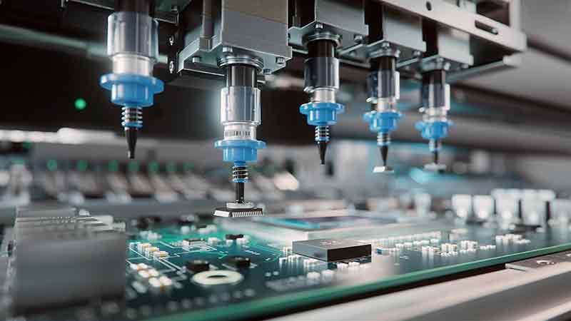
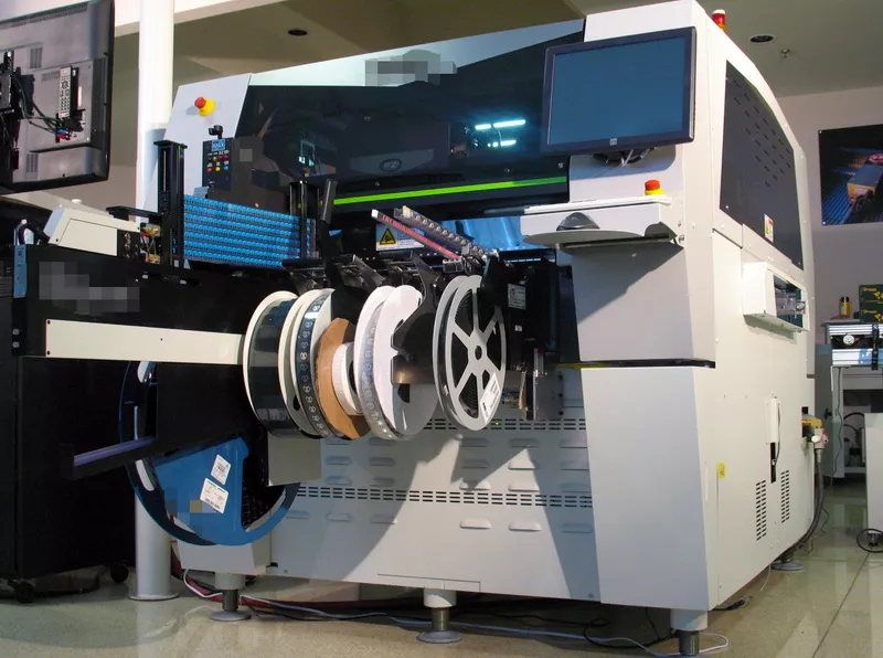
Pick and place machines, core to surface-mount technology (SMT), use robotic arms equipped with vacuum nozzles to retrieve components from feeders and deposit them onto PCB pads. In prototype assembly, these machines excel in handling small quantities, making pick and place for small runs highly efficient. Unlike high-volume production lines, prototypes often involve unique boards with varied component types, where manual assembly risks inconsistencies. These machines integrate vision systems for alignment, ensuring components land exactly where needed before reflow soldering. For electrical engineers, this matters because it aligns with the need for rapid PCB prototyping, allowing focus on functionality testing rather than placement errors. Adopting such automation minimizes defects that could derail early-stage evaluations.
Key Advantages of Pick and Place Machines in Prototype Assembly
One primary advantage lies in the unparalleled precision these machines offer for pick and place prototype assembly. Advanced vision cameras detect fiducials and component leads, compensating for minor board warpage or misalignment down to microns. This level of accuracy surpasses hand placement, where human fatigue leads to offsets exceeding tolerances. Engineers achieve consistent pad-to-component alignment, crucial for signal integrity in high-density designs. Such precision reduces post-assembly rework, saving valuable prototyping cycles.
Speed represents another compelling benefit, particularly for SMT prototypes requiring quick assembly. Modern machines place thousands of components per hour, even in small runs, far outpacing manual methods. Setup times have shortened with intuitive software interfaces that import CAD files directly for programming. This enables rapid PCB prototyping workflows, where a board assembles in minutes rather than hours. For teams iterating designs weekly, this acceleration directly impacts project timelines and resource allocation.
Consistency across multiple boards emerges as a standout feature in pick and place for small runs. Once programmed, the machine repeats placements identically, eliminating variability from operator skill differences. This repeatability proves vital for prototype PCB assembly, where engineers need reliable baselines for performance comparisons. Batches of 5 to 50 units maintain uniform quality, facilitating statistical analysis of electrical characteristics. Over time, this builds confidence in scaling to production.
Technical Principles Behind Effective Pick and Place Operation
Pick and place machines operate on a gantry or turret system, where heads pick components via nozzles calibrated to part sizes. Feeders, ranging from tape to tray types, supply parts in bulk, with intelligent systems verifying orientation through upward-facing cameras. Placement occurs after downward vision confirmation, aligning to pad centroids per design files. Factors like nozzle vacuum pressure and Z-axis control ensure gentle handling, preventing damage to delicate leads. Engineers must consider component pitch and board size limits when selecting machines for prototype work. These principles, characterized under IPC-9850 standards for placement equipment, guide performance benchmarking.
Flexibility in handling diverse components sets these machines apart for rapid PCB prototyping. Quick-change nozzles and feeder swaps accommodate resistors, ICs, and odd-form parts without extensive downtime. Software supports mixed-technology boards, blending SMT with through-hole if needed. This adaptability suits prototype phases, where designs evolve frequently. Engineers program offsets for non-standard packages, ensuring versatility across projects.
Cost-Effectiveness and Reduced Errors in Small-Run Scenarios
For pick and place for small runs, cost-effectiveness stems from low per-board expenses compared to outsourcing or manual labor. Amortized setup costs drop with efficient programming tools that reuse libraries for common parts. No labor scaling issues arise, as one operator oversees multiple machines. This makes prototype PCB assembly economical even for one-off boards. Long-term, fewer defects translate to savings on scrap and debugging.
Human error reduction stands as a major advantage, with automation eliminating placement offsets, polarity mistakes, and tombstoning precursors. Vision-guided systems flag anomalies pre-placement, alerting operators to feeder jams or wrong parts. Statistical process control logs data for traceability, aiding root-cause analysis. In high-reliability prototypes, this aligns with IPC-A-610 acceptability criteria for electronic assemblies, ensuring class 2 or 3 compliance from the start.
Best Practices for Optimizing Pick and Place Prototype Assembly
Start with accurate Gerber and BOM files, verifying component footprints against datasheets to avoid mismatches. Calibrate the machine daily, using test boards to confirm accuracy within specified tolerances. Organize feeders by part type, prioritizing high-use components in fast-access positions. Run dry cycles first to detect programming errors without wasting boards. Post-placement, inspect via automated optical systems before reflow, adhering to J-STD-001 requirements for soldered assemblies. These steps maximize uptime and yield in rapid PCB prototyping.
Panelize designs judiciously for prototypes, balancing machine throughput with depaneling ease. Use fiducials at board corners and centers for robust alignment, especially on flexible substrates. Optimize placement sequences to minimize head travel, boosting speed for small runs. Maintain clean environments to prevent contamination affecting vacuum pick-up. Document all parameters for repeatability across revisions.
Troubleshooting Common Issues in Pick and Place Operations
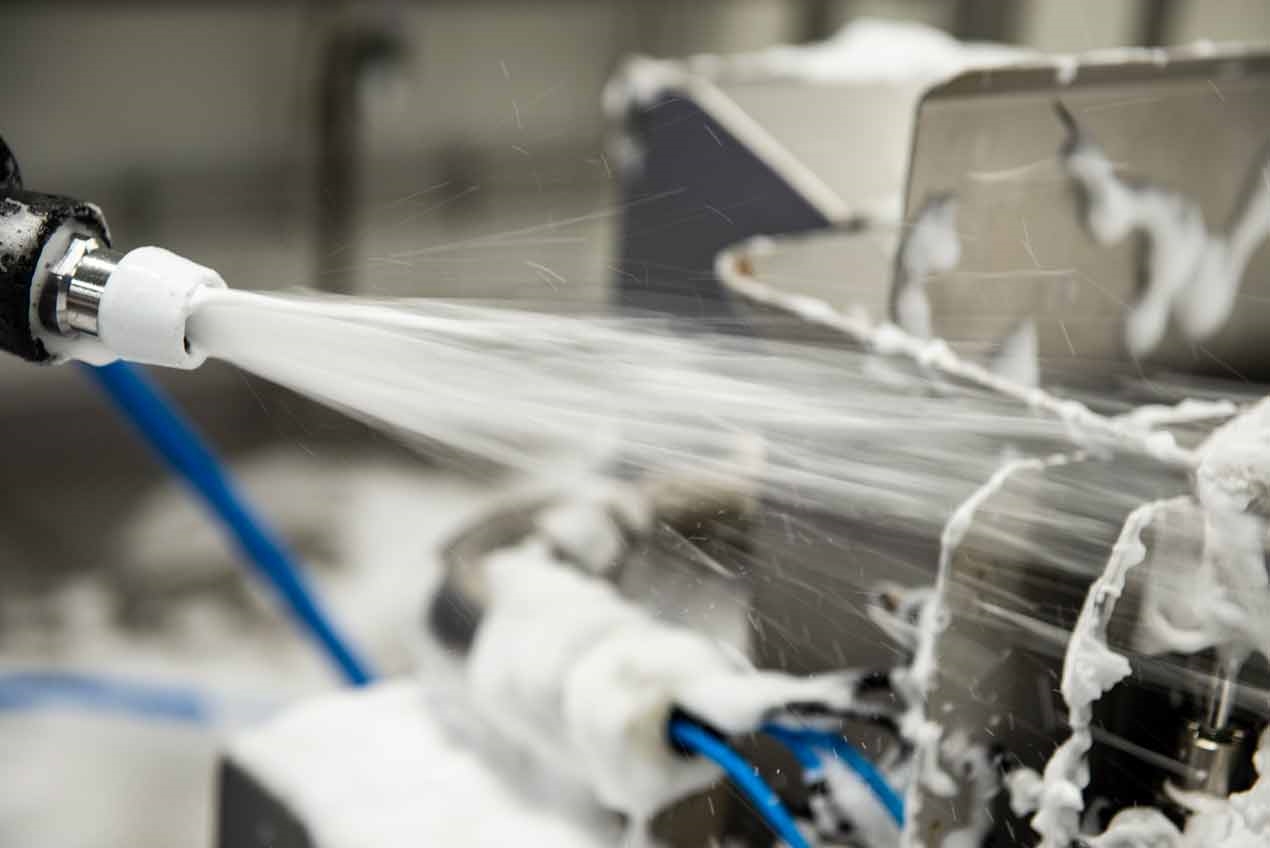
Feeder jams often occur from tangled tape or dust; regular cleaning and tension checks prevent this. If placements skew, verify machine leveling and vision calibration, as thermal expansion can shift references. Component tombstoning post-reflow traces back to uneven paste deposition, not placement, but pre-check paste volume. Polarity errors signal feeder orientation issues; double-verify part numbers during setup. For fine-pitch parts, nozzle wear causes misses, so inspect and rotate regularly. These practical fixes keep prototype PCB assembly on track.
Missed picks from vacuum loss demand pressure gauge monitoring and filter changes. Software glitches arise from corrupted fiducials; regenerate from CAD if needed. Overly dense boards strain throughput, so simulate paths beforehand. Log errors for pattern recognition, refining future runs. This troubleshooting mindset ensures reliable pick and place prototype assembly.
Conclusion
Pick and place machines deliver transformative advantages for prototype PCB assembly, from precision and speed to consistency and cost savings. Electrical engineers gain a powerful tool for rapid PCB prototyping, handling small runs with production-like quality. By leveraging vision systems, flexible feeders, and best practices, teams minimize errors and accelerate development. Standards like IPC-9850, IPC-A-610, and J-STD-001 provide the framework for excellence. Ultimately, integrating these machines empowers innovation, bridging prototypes to viable products efficiently.
FAQs
Q1: What is pick and place prototype assembly, and how does it differ from manual methods?
A1: Pick and place prototype assembly uses automated machines to position SMT components precisely on PCBs for small batches. Unlike manual soldering, which relies on operator skill and fatigues quickly, machines employ vision systems for micron-level accuracy and repeatability. This suits rapid PCB prototyping, reducing errors like misalignment or polarity issues. Engineers achieve consistent results across boards, aligning with IPC-A-610 criteria without extensive training.
Q2: Why choose pick and place machines for small runs in SMT prototypes?
A2: Pick and place for small runs offers cost-effective automation without high-volume setup costs, placing components faster than hand assembly. Flexibility in handling varied parts supports iterative designs in prototype PCB assembly. Vision-guided placement ensures adherence to tolerances, minimizing rework. This approach accelerates timelines while maintaining quality for electrical testing.
Q3: How do pick and place machines support rapid PCB prototyping workflows?
A3: These machines import design files for quick programming, enabling assembly of SMT prototypes in hours. Quick feeder changes and nozzle swaps handle design revisions seamlessly. Post-placement inspections catch issues early, per J-STD-001 guidelines. Engineers focus on validation rather than labor-intensive placement, streamlining the prototyping cycle.
Q4: What are common benefits of prototype PCB assembly with pick and place technology?
A4: Benefits include high precision reducing defects, speed for faster iterations, and consistency for reliable testing. Cost savings emerge from low per-unit expenses in small runs. Error reduction via automation boosts yield, supporting complex designs. This technology aligns with industry standards for professional-grade prototypes.
References
IPC-9850A — Surface Mount Placement Equipment Characterization. IPC, 2011
IPC-A-610H — Acceptability of Electronic Assemblies. IPC, 2019
J-STD-001H — Requirements for Soldered Electrical and Electronic Assemblies. IPC/JEDEC, 2018