 ALLPCB


Introduction
PCB panelization allows multiple individual boards to be fabricated together on a single larger panel. This approach improves manufacturing efficiency and reduces handling costs during production. Engineers use Altium PCB design tools to define the panel layout before sending files to fabrication. The process incorporates features such as step and repeat arrays and embedded board arrays to maintain precise alignment and spacing. Proper panel creation also supports downstream assembly steps while meeting quality expectations outlined in industry standards.
What Is PCB Panelization and Why It Matters
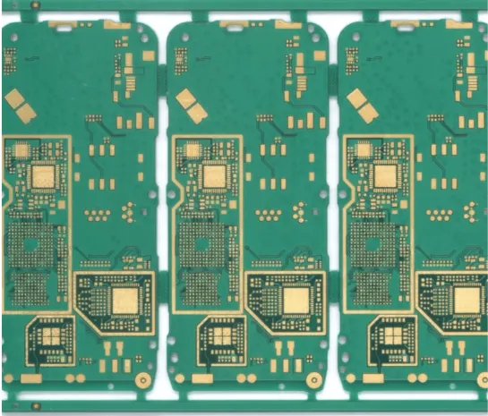
PCB panelization refers to the arrangement of multiple printed circuit boards onto one larger substrate known as a panel. This technique is commonly implemented through Altium embedded board array or Altium step and repeat functions. It enables fabricators to process several designs in a single run, which lowers per-unit costs and simplifies material handling.
Panelization also improves mechanical stability during etching, drilling, and plating operations. Without it, thin or small boards can warp or become difficult to process individually. The practice aligns with established quality expectations in IPC-6012E, which addresses qualification and performance requirements for rigid printed boards. Overall, effective panel design contributes to higher yield rates and consistent board quality across production batches.
Technical Principles of PCB Panel Creation
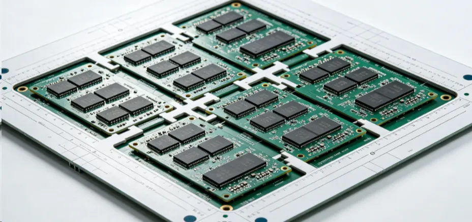
Panel creation begins with defining the individual board outline and then replicating it across the panel area. Spacing between boards must account for routing or scoring allowances, typically 2 to 3 millimeters depending on the separation method. Tooling holes, fiducial marks, and breakaway tabs are added to maintain registration and facilitate depanelization after fabrication.
Engineers must consider copper balance, thermal expansion, and mechanical stress to prevent warpage. IPC-A-600K provides acceptability criteria for printed boards, including guidance on surface finish, hole quality, and laminate integrity that indirectly influence panel layout decisions. Step and repeat patterns ensure uniform distribution while leaving sufficient margins for handling rails. These rails often include additional copper or non-functional areas that absorb mechanical stress during processing. Accurate implementation of these principles reduces defects and supports reliable assembly later in the workflow.
Practical Solutions and Best Practices in Altium Designer
Begin by opening the existing PCB design file and verifying that the board outline and layer stackup are complete. Access the panelization tools to create an embedded board array or apply step and repeat commands. Specify the number of columns and rows, along with horizontal and vertical spacing values that match fabrication requirements.
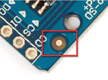
Next, add panel borders or rails on the mechanical layer to define the overall panel dimensions. Place tooling holes at the corners or edges according to the fabricator’s specifications, usually 3.175 millimeters in diameter. Insert fiducial marks on the top and bottom copper layers for optical alignment during assembly.
Review the panel for copper distribution balance and ensure no overlapping features exist between adjacent boards. Generate manufacturing outputs including Gerber files, drill files, and a panel drawing that clearly shows dimensions and reference points. Always cross-check the layout against IPC-A-600K acceptability criteria before finalizing the design package.
These steps produce a panel that fabricators can process efficiently while maintaining traceability and dimensional accuracy throughout production.
Conclusion
Creating a well-designed PCB panel in Altium Designer streamlines fabrication and supports consistent quality. By following structured steps for array definition, spacing, and feature placement, engineers achieve reliable results that meet both functional and manufacturing needs. Attention to industry standards such as IPC-6012E and IPC-A-600K helps ensure the final boards perform as intended after depanelization. This methodical approach reduces rework and contributes to smoother transitions from design to production.
FAQs
Q1: What does an Altium PCB panelization tutorial typically cover?
A1: An Altium PCB panelization tutorial explains how to arrange multiple boards into a single panel using embedded board array and step and repeat features. It covers spacing rules, tooling hole placement, fiducial positioning, and output generation. The guidance emphasizes maintaining design integrity while optimizing for manufacturing efficiency and compliance with IPC standards.
Q2: How does Altium embedded board array differ from simple step and repeat?
A2: Altium embedded board array allows complex nesting of boards with varying orientations within the panel. Step and repeat creates a uniform grid of identical boards. Both methods support panel creation, but the embedded array offers greater flexibility for mixed designs or irregular shapes while still requiring proper clearance and alignment features.
Q3: Why is create PCB panel an important step in Altium PCB design?
A3: Creating a PCB panel early in the design process ensures that manufacturing constraints are addressed before files are released. It allows verification of spacing, rail design, and registration features that affect yield and cost. Proper panelization also simplifies assembly processes by providing consistent handling surfaces and alignment marks.
Q4: What are common considerations when using Altium step and repeat for panels?
A4: Common considerations include setting accurate row and column counts, defining sufficient spacing for routing or scoring, and adding rails for mechanical stability. Engineers must also place fiducials and tooling holes consistently and verify copper balance across the panel. These steps help prevent warpage and ensure compatibility with fabrication equipment.
References
IPC-6012E — Qualification and Performance Specification for Rigid Printed Boards. IPC, 2017
IPC-A-600K — Acceptability of Printed Boards. IPC, 2020





