 ALLPCB


Silkscreen Font Size for Beginners: A Hobbyist's Guide to PCB Marking
Silkscreen markings play an essential role in DIY PCB projects by providing clear labels for components, pinouts, and warnings. Hobbyists working on home etching PCB boards rely on these markings to simplify assembly and reduce errors during testing. Proper font choices ensure that text remains legible even after the board undergoes etching and soldering processes. Selecting an appropriate silkscreen font size helps maintain readability without crowding the limited space on compact layouts. This guide focuses on practical considerations for hobbyist PCB marking to support successful builds.
What Is PCB Silkscreen and Why It Matters for Hobbyists
PCB silkscreen refers to the non-conductive ink layer applied to the board surface that carries text, symbols, and graphics. In DIY PCB silkscreen work, this layer identifies component locations and orientations, making it easier to place parts correctly during manual assembly. Clear markings also support troubleshooting when circuits do not function as expected. For hobbyists engaged in home etching PCB projects, effective silkscreen improves the overall usability of the finished board. Industry standards such as those outlined in IPC-A-600 emphasize the need for legible markings to meet basic acceptability criteria for printed boards.
The choice of font size directly influences how well markings perform in real-world use. Text that is too small becomes difficult to read under typical workshop lighting, while overly large fonts may overlap traces or pads. Hobbyists often balance these factors when designing boards for personal projects or small-scale prototypes. Consistent application of simple PCB labels helps maintain organization throughout the build process.
Technical Principles Behind Effective Silkscreen Font Selection
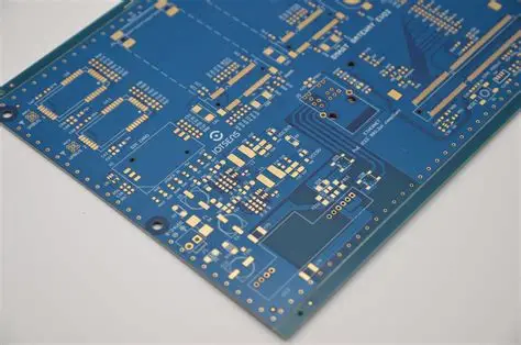
Silkscreen text must maintain sufficient contrast against the board substrate and solder mask to remain visible after fabrication. Sans-serif fonts generally provide better clarity than decorative styles because their uniform stroke widths reduce visual distortion during printing or transfer. The physical dimensions of the board, the density of nearby traces, and the intended viewing distance all influence how text appears once applied. In hobbyist PCB marking, these elements combine to determine whether markings support quick identification or require magnification.
Manufacturing methods common in home settings, such as toner transfer or direct printing, can affect edge sharpness and ink adhesion. Standards from IPC-6012 highlight performance expectations for rigid boards, including the durability of surface markings under typical handling conditions. Font weight and character spacing further contribute to overall legibility, especially when multiple lines of text appear in close proximity. Hobbyists benefit from testing sample prints on scrap material to observe how different font configurations behave after etching.
Practical Solutions and Best Practices for Hobbyists
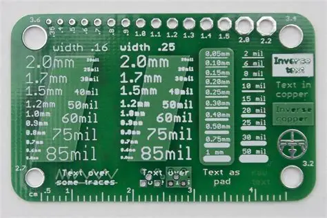
Begin by selecting a clean, widely available sans-serif typeface that renders consistently across design software and transfer methods. Maintain uniform line thickness throughout characters to avoid thin strokes that may disappear during the etching stage. Position text away from high-density areas to prevent interference with electrical paths while preserving adequate space for component outlines.
Review the full layout at actual size before finalizing the design to confirm that all simple PCB labels remain distinguishable. When working with DIY PCB silkscreen techniques, apply the ink layer after etching but before soldering to minimize handling damage. Multiple light passes or adjusted exposure settings during transfer can improve ink density and edge definition on home setups.
Document the chosen font parameters for each project so that future revisions maintain consistency. This approach supports repeatable results across successive boards without unnecessary trial and error.
Troubleshooting Common Silkscreen Issues in Home Projects
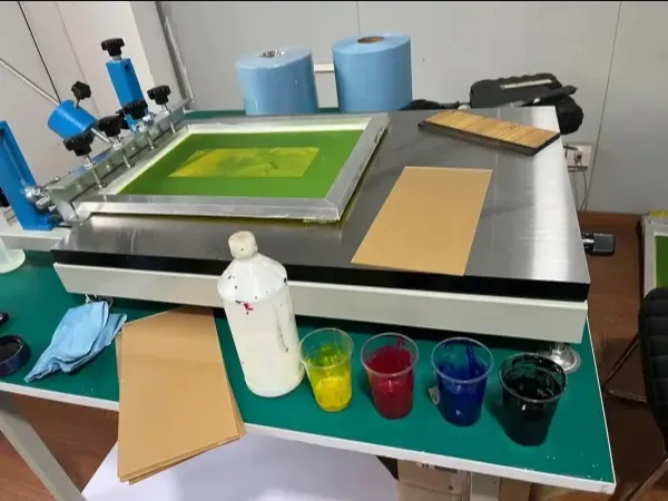
When text appears faint after transfer, increasing ink volume or adjusting pressure during the application step often restores visibility. Overlapping characters usually result from insufficient spacing, which can be corrected by expanding character kerning in the design file. Boards that experience minor warpage during etching may distort fine details, so verifying flatness before marking helps preserve clarity.
If labels become partially obscured by solder mask bleed, reviewing mask alignment prior to application prevents recurrence. Hobbyists frequently resolve these issues through iterative testing on small sections of board material. Consistent attention to these details strengthens the reliability of hobbyist PCB marking across different project scales.
Conclusion
Effective silkscreen font choices enhance the functionality and readability of DIY PCB projects by ensuring that essential markings remain clear throughout assembly and use. Attention to typeface style, placement, and contrast supports better outcomes in home etching PCB workflows. Following established practices aligned with relevant industry standards reduces common errors and improves overall project success. Hobbyists who apply these principles consistently produce boards that are easier to work with and maintain.
FAQs
Q1: What font characteristics work best for DIY PCB silkscreen on small boards?
A1: Sans-serif fonts with consistent stroke widths provide reliable clarity when space is limited. Hobbyists achieve good results by testing sample transfers on scrap material before committing to the final design. This approach helps maintain legibility without crowding other board features.
Q2: How does hobbyist PCB marking improve assembly accuracy during home projects?
A2: Clear component labels and orientation markers reduce placement mistakes and speed up manual soldering. Simple PCB labels also assist with later modifications or repairs by identifying connections quickly. Consistent marking practices support more efficient workflow from design through testing.
Q3: Why should easy silkscreen font sizes be verified before etching a full board?
A3: Verification at actual size reveals whether text remains readable after the transfer and etching steps. Adjustments made early prevent wasted material and time on boards that require rework. This step proves especially useful when working with compact layouts common in hobbyist designs.
Q4: What role do industry standards play in hobbyist PCB marking decisions?
A4: Standards such as those in IPC-A-600 provide guidance on acceptable marking quality for printed boards. Hobbyists who reference these expectations can align their work with recognized criteria for legibility and durability. Applying such principles helps produce boards that meet basic professional benchmarks even in home settings.
References
IPC-A-600K — Acceptability of Printed Boards. IPC, 2020
IPC-6012E — Qualification and Performance Specification for Rigid Printed Boards. IPC, 2017





