 ALLPCB


What Is Double-Sided PCB Silkscreen and Why It Matters
Double-sided PCB silkscreen refers to the application of ink-based markings on both surfaces of a board that contains copper traces and components on two sides. This approach differs from single-sided designs because the top and bottom layers must coordinate without interfering with vias, pads, or routing. Silkscreen on both sides improves component identification during assembly and supports troubleshooting after installation.
Industry professionals rely on balanced silkscreen design to reduce placement errors and meet quality expectations. Poor coordination between layers can lead to misaligned text, obscured features, or ink that interferes with soldering. Proper planning ensures the markings remain functional throughout the product life cycle.
Technical Principles of Silkscreen Application on Double-Sided Boards
Silkscreen application begins with artwork generation in the design files, followed by printing or imaging onto the solder mask surfaces. On double-sided boards, registration between the top and bottom layers requires precise alignment to prevent text from overlapping copper features or falling into non-copper areas. The ink must adhere reliably to the solder mask while withstanding subsequent thermal and chemical processes.
Key mechanisms include layer-to-layer registration accuracy and ink thickness control. Thermal expansion of the base material during curing or reflow can shift features slightly, affecting text placement. Designers account for these effects by maintaining adequate clearance around pads and traces. IPC-A-600 outlines acceptability criteria for silkscreen quality, including legibility and adhesion.
Component placement on double-sided PCBs influences silkscreen positioning because parts mounted on one side may shadow or conflict with markings on the opposite side. Vias that connect the two sides also require clearance zones so that silkscreen does not bridge or contaminate them. These interactions demand coordinated layout decisions early in the design phase.
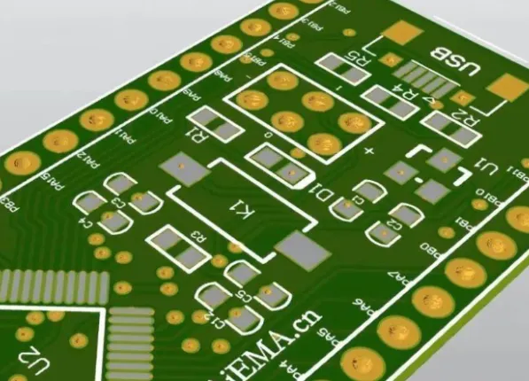
Practical Solutions and Best Practices for Balanced Design
Designers achieve balance by establishing consistent rules for text size, font style, and orientation across both layers. Text should remain horizontal or follow board edges where possible to aid readability during assembly and inspection. Minimum line widths and character heights follow manufacturer guidelines to ensure the ink prints cleanly without bleeding.
Clearance requirements prevent silkscreen from encroaching on pads, traces, or fiducials. A common approach places all component designators on the top layer when feasible, while using the bottom layer for supplementary information such as board revision or serial number fields. When markings must appear on both sides, mirrored or offset positioning avoids direct overlap through the board thickness.
Coordination with the fabrication process helps resolve potential conflicts. Early review of stack-up and mask properties allows adjustments before artwork finalization. IPC-6012 provides qualification guidance that supports consistent silkscreen performance across production lots.
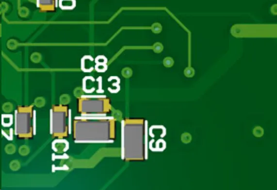
Additional practices include selecting ink colors that contrast well with the solder mask and verifying that bottom-side text remains visible after component placement. Avoiding dense clusters of text near high-density areas reduces the risk of partial coverage. These steps collectively improve first-pass yield during assembly.
Troubleshooting Common Silkscreen Issues in Double-Sided Designs
Misalignment between top and bottom silkscreen often appears as text shifted relative to component outlines. This condition typically stems from registration tolerances during imaging or material movement. Reviewing layer alignment in the design files and confirming panelization methods helps identify the source.
Ink smearing or poor adhesion may occur when silkscreen overlaps areas subjected to mechanical stress or repeated thermal cycling. Adjusting clearance rules and verifying mask compatibility during the quoting stage minimizes these occurrences. In cases of persistent issues, designers may simplify bottom-layer markings to essential identifiers only.
Conclusion
Balanced silkscreen design on double-sided PCBs requires attention to registration, clearance, and layer coordination from the earliest layout stages. These practices support reliable component placement, accurate assembly, and effective field service. Following established industry guidelines helps maintain consistent quality across production.
FAQs
Q1: What are the main challenges when applying silkscreen on both sides of a double-sided PCB?
A1: The primary challenges involve maintaining precise layer-to-layer registration while ensuring text does not overlap copper features or interfere with assembly processes. Designers must also consider thermal effects and ink adhesion on both surfaces. Addressing these factors early supports higher manufacturing yields and clearer component identification.
Q2: How does silkscreen design influence component placement on double-sided PCBs?
A2: Silkscreen placement affects component orientation and spacing because markings must remain visible and unobstructed. Adequate clearance around pads and vias allows components to sit correctly without covering critical labels. Coordinated top and bottom designs reduce the likelihood of placement errors during automated assembly.
Q3: What design rules help achieve balanced silkscreen on double-sided boards?
A3: Effective rules include consistent text sizing, sufficient clearance from copper, and selective use of bottom-layer markings. Horizontal orientation and contrasting colors improve readability. Early collaboration on fabrication capabilities ensures the chosen rules align with process limits.
Q4: Why is silkscreen balance important for double-sided PCB manufacturing?
A4: Balanced silkscreen supports accurate assembly, simplifies inspection, and aids troubleshooting throughout the product life. It reduces the chance of misinterpretation during placement and helps meet overall board quality expectations. Proper design minimizes rework and supports reliable end-product performance.
References
IPC-A-600K - Acceptability of Printed Boards. IPC, 2020
IPC-6012E - Qualification and Performance Specification for Rigid Printed Boards. IPC, 2017





